
Datasheet
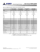
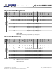

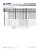

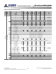
Table Of Contents
- DDR3L SDRAM
- Description
- State Diagram
- Functional Description
- Functional Block Diagrams
- Ball Assignments and Descriptions
- Package Dimensions
- Electrical Specifications
- Thermal Characteristics
- Electrical Specifications – I DD Specifications and Conditions
- Electrical Characteristics – 1.35V IDD Specifications
- Electrical Specifications – DC and AC
- ODT Characteristics
- Output Driver Impedance
- Output Characteristics and Operating Conditions
- Speed Bin Tables
- Electrical Characteristics and AC Operating Conditions
- Electrical Characteristics and AC Operating Conditions
- Command and Address Setup, Hold, and Derating
- Data Setup, Hold, and Derating
- Commands – Truth Tables
- Commands
- Input Clock Frequency Change
- Write Leveling
- Initialization
- Voltage Initialization / Change
- Mode Registers
- Mode Register 0 (MR0)
- Mode Register 1 (MR1)
- Mode Register 2 (MR2)
- Mode Register 3 (MR3)
- MODE REGISTER SET (MRS) Command
- ZQ CALIBRATION Operation
- ACTIVATE Operation
- READ Operation
- WRITE Operation
- PRECHARGE Operation
- SELF REFRESH Operation
- Extended Temperature Usage
- Power-Down Mode
- RESET Operation
- On-Die Termination (ODT)
- Dynamic ODT
- Synchronous ODT Mode
- Asynchronous ODT Mode
- Asynchronous to Synchronous ODT Mode Transition (Power-Down Exit)
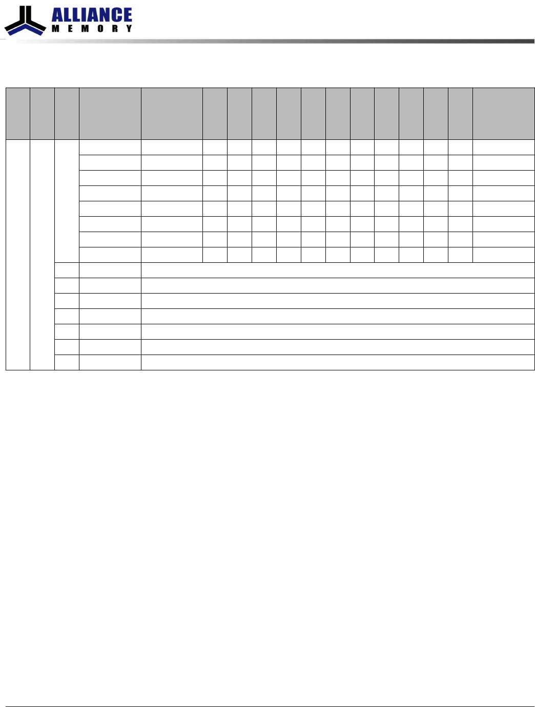
Table 14: I
DD4R
Measurement Loop
CK, CK#
CKE
Sub-Loop
Cycle
Number
Command
CS#
RAS#
CAS#
WE#
ODT
BA[2:0]
A[15:11]
A[10]
A[9:7]
A[6:3]
A[2:0]
Data
3
Toggling
Static HIGH
0
0 RD 0 1 0 1 0 0 0 0 0 0 0 00000000
1 D 10000000000 –
2 D# 11110000000 –
3 D# 11110000000 –
4 RD 0 1 0 1 0 0 0 0 0 F 0 00110011
5 D 100000000F0 –
6 D# 111100000F0 –
7 D# 111100000F0 –
1 8–15 Repeat sub-loop 0, use BA[2:0] = 1
2 16–23 Repeat sub-loop 0, use BA[2:0] = 2
3 24–31 Repeat sub-loop 0, use BA[2:0] = 3
4 32–39 Repeat sub-loop 0, use BA[2:0] = 4
5 40–47 Repeat sub-loop 0, use BA[2:0] = 5
6 48–55 Repeat sub-loop 0, use BA[2:0] = 6
7 56–63 Repeat sub-loop 0, use BA[2:0] = 7
Notes:
1. DQ, DQS, DQS# are midlevel when not driving in burst sequence.
2. DM is LOW.
3. Burst sequence is driven on each DQ signal by the RD command.
4. All banks open.
8Gb: x4, x8, x16 DDR3L SDRAM
Electrical Specifications – I
DD
Specifications and Conditions
32
Rev.2.0 June 2016
© 2015 Alliance Memory, Inc. All rights reserved.
Alliance Memory Inc. reserves the right to change products or specification without notice
Alliance Memory Inc. 511 Taylor Way, San Carlos, CA 94070
TEL: (650) 610-6800 FAX: (650) 620-9211