
Datasheet
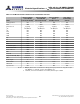


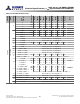
Table Of Contents
- DDR3L SDRAM
- Description
- State Diagram
- Functional Description
- Functional Block Diagrams
- Ball Assignments and Descriptions
- Package Dimensions
- Electrical Specifications
- Thermal Characteristics
- Electrical Specifications – I DD Specifications and Conditions
- Electrical Characteristics – 1.35V IDD Specifications
- Electrical Specifications – DC and AC
- ODT Characteristics
- Output Driver Impedance
- Output Characteristics and Operating Conditions
- Speed Bin Tables
- Electrical Characteristics and AC Operating Conditions
- Electrical Characteristics and AC Operating Conditions
- Command and Address Setup, Hold, and Derating
- Data Setup, Hold, and Derating
- Commands – Truth Tables
- Commands
- Input Clock Frequency Change
- Write Leveling
- Initialization
- Voltage Initialization / Change
- Mode Registers
- Mode Register 0 (MR0)
- Mode Register 1 (MR1)
- Mode Register 2 (MR2)
- Mode Register 3 (MR3)
- MODE REGISTER SET (MRS) Command
- ZQ CALIBRATION Operation
- ACTIVATE Operation
- READ Operation
- WRITE Operation
- PRECHARGE Operation
- SELF REFRESH Operation
- Extended Temperature Usage
- Power-Down Mode
- RESET Operation
- On-Die Termination (ODT)
- Dynamic ODT
- Synchronous ODT Mode
- Asynchronous ODT Mode
- Asynchronous to Synchronous ODT Mode Transition (Power-Down Exit)
Table 11: I
DD
Measurement Conditions for Power-Down Currents
Name
I
DD2P0
Precharge
Power-Down
Current (Slow Exit)
1
I
DD2P1
Precharge
Power-Down
Current (Fast Exit)
1
I
DD2Q
Precharge
Quiet
Standby Current
I
DD3P
Active
Power-Down
Current
Timing pattern N/A N/A N/A N/A
CKE LOW LOW HIGH LOW
External clock Toggling Toggling Toggling Toggling
t
CK
t
CK (MIN) I
DD
t
CK (MIN) I
DD
t
CK (MIN) I
DD
t
CK (MIN) I
DD
t
RC N/A N/A N/A N/A
t
RAS N/A N/A N/A N/A
t
RCD N/A N/A N/A N/A
t
RRD N/A N/A N/A N/A
t
RC N/A N/A N/A N/A
CL N/A N/A N/A N/A
AL N/A N/A N/A N/A
CS# HIGH HIGH HIGH HIGH
Command inputs LOW LOW LOW LOW
Row/column addr LOW LOW LOW LOW
Bank addresses LOW LOW LOW LOW
DM LOW LOW LOW LOW
Data I/O Midlevel Midlevel Midlevel Midlevel
Output buffer DQ, DQS Enabled Enabled Enabled Enabled
ODT
2
Enabled, off Enabled, off Enabled, off Enabled, off
Burst length 8 8 8 8
Active banks None None None All
Idle banks All All All None
Special notes N/A N/A N/A N/A
Notes:
1. MR0[12] defines DLL on/off behavior during precharge power-down only; DLL on (fast
exit, MR0[12] = 1) and DLL off (slow exit, MR0[12] = 0).
2. “Enabled, off” means the MR bits are enabled, but the signal is LOW.
8Gb: x4, x8, x16 DDR3L SDRAM
Electrical Specifications – I
DD
Specifications and Conditions
30
Rev.2.0 June 2016
© 2015 Alliance Memory, Inc. All rights reserved.
Alliance Memory Inc. reserves the right to change products or specification without notice
Alliance Memory Inc. 511 Taylor Way, San Carlos, CA 94070
TEL: (650) 610-6800 FAX: (650) 620-9211