
Datasheet
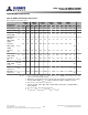
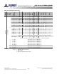
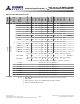
Table Of Contents
- DDR3L SDRAM
- Description
- State Diagram
- Functional Description
- Functional Block Diagrams
- Ball Assignments and Descriptions
- Package Dimensions
- Electrical Specifications
- Thermal Characteristics
- Electrical Specifications – I DD Specifications and Conditions
- Electrical Characteristics – 1.35V IDD Specifications
- Electrical Specifications – DC and AC
- ODT Characteristics
- Output Driver Impedance
- Output Characteristics and Operating Conditions
- Speed Bin Tables
- Electrical Characteristics and AC Operating Conditions
- Electrical Characteristics and AC Operating Conditions
- Command and Address Setup, Hold, and Derating
- Data Setup, Hold, and Derating
- Commands – Truth Tables
- Commands
- Input Clock Frequency Change
- Write Leveling
- Initialization
- Voltage Initialization / Change
- Mode Registers
- Mode Register 0 (MR0)
- Mode Register 1 (MR1)
- Mode Register 2 (MR2)
- Mode Register 3 (MR3)
- MODE REGISTER SET (MRS) Command
- ZQ CALIBRATION Operation
- ACTIVATE Operation
- READ Operation
- WRITE Operation
- PRECHARGE Operation
- SELF REFRESH Operation
- Extended Temperature Usage
- Power-Down Mode
- RESET Operation
- On-Die Termination (ODT)
- Dynamic ODT
- Synchronous ODT Mode
- Asynchronous ODT Mode
- Asynchronous to Synchronous ODT Mode Transition (Power-Down Exit)
Electrical Specifications
Absolute Ratings
Stresses greater than those listed may cause permanent damage to the device. This is a
stress rating only, and functional operation of the device at these or any other condi-
tions outside those indicated in the operational sections of this specification is not im-
plied. Exposure to absolute maximum rating conditions for extended periods may ad-
versely affect reliability.
Table 5: Absolute Maximum Ratings
Symbol Parameter Min Max Unit Notes
V
DD
V
DD
supply voltage relative to V
SS
–0.4 1.975 V 1
V
DDQ
V
DD
supply voltage relative to V
SSQ
–0.4 1.975 V
V
IN
, V
OUT
Voltage on any pin relative to V
SS
–0.4 1.975 V
T
C
Operating case temperature – Commercial 0 95 °C 2, 3
Operating case temperature – Industrial –40 95 °C 2, 3
T
STG
Storage temperature –55 150 °C
Notes:
1. V
DD
and V
DDQ
must be within 300mV of each other at all times, and V
REF
must not be
greater than 0.6 × V
DDQ
. When V
DD
and V
DDQ
are <500mV, V
REF
can be ≤300mV.
2. MAX operating case temperature. T
C
is measured in the center of the package.
3. Device functionality is not guaranteed if the DRAM device exceeds the maximum T
C
dur-
ing operation.
8Gb: x4, x8, x16 DDR3L SDRAM
Electrical Specifications
24
Rev.2.0 June 2016
© 2015 Alliance Memory, Inc. All rights reserved.
Alliance Memory Inc. reserves the right to change products or specification without notice
Alliance Memory Inc. 511 Taylor Way, San Carlos, CA 94070
TEL: (650) 610-6800 FAX: (650) 620-9211