
Datasheet
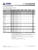
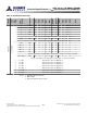
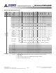
Table Of Contents
- DDR3L SDRAM
- Description
- State Diagram
- Functional Description
- Functional Block Diagrams
- Ball Assignments and Descriptions
- Package Dimensions
- Electrical Specifications
- Thermal Characteristics
- Electrical Specifications – I DD Specifications and Conditions
- Electrical Characteristics – 1.35V IDD Specifications
- Electrical Specifications – DC and AC
- ODT Characteristics
- Output Driver Impedance
- Output Characteristics and Operating Conditions
- Speed Bin Tables
- Electrical Characteristics and AC Operating Conditions
- Electrical Characteristics and AC Operating Conditions
- Command and Address Setup, Hold, and Derating
- Data Setup, Hold, and Derating
- Commands – Truth Tables
- Commands
- Input Clock Frequency Change
- Write Leveling
- Initialization
- Voltage Initialization / Change
- Mode Registers
- Mode Register 0 (MR0)
- Mode Register 1 (MR1)
- Mode Register 2 (MR2)
- Mode Register 3 (MR3)
- MODE REGISTER SET (MRS) Command
- ZQ CALIBRATION Operation
- ACTIVATE Operation
- READ Operation
- WRITE Operation
- PRECHARGE Operation
- SELF REFRESH Operation
- Extended Temperature Usage
- Power-Down Mode
- RESET Operation
- On-Die Termination (ODT)
- Dynamic ODT
- Synchronous ODT Mode
- Asynchronous ODT Mode
- Asynchronous to Synchronous ODT Mode Transition (Power-Down Exit)
Table 4: 96-Ball FBGA – x16 Ball Descriptions
Symbol Type Description
A[15:13], A12/BC#,
A11, A10/AP, A[9:0]
Input Address inputs: Provide the row address for ACTIVATE commands, and the column
address and auto precharge bit (A10) for READ/WRITE commands, to select one
location out of the memory array in the respective bank. A10 sampled during a
PRECHARGE command determines whether the PRECHARGE applies to one bank
(A10 LOW, bank selected by BA[2:0]) or all banks (A10 HIGH). The address inputs also
provide the op-code during a LOAD MODE command. Address inputs are referenced
to V
REFCA
. A12/BC#: When enabled in the mode register (MR), A12 is sampled during
READ and WRITE commands to determine whether burst chop (on-the-fly) will be
performed (HIGH = BL8 or no burst chop, LOW = BC4). See the Truth Table – Com-
mand section.
BA[2:0] Input Bank address inputs: BA[2:0] define the bank to which an ACTIVATE, READ,
WRITE, or PRECHARGE command is being applied. BA[2:0] define which mode
register (MR0, MR1, MR2, or MR3) is loaded during the LOAD MODE command.
BA[2:0] are referenced to V
REFCA
.
CK, CK# Input Clock: CK and CK# are differential clock inputs. All control and address input signals
are sampled on the crossing of the positive edge of CK and the negative edge of
CK#. Output data strobe (DQS, DQS#) is referenced to the crossings of CK and CK#.
CKE Input Clock enable: CKE enables (registered HIGH) and disables (registered LOW) internal
circuitry and clocks on the DRAM. The specific circuitry that is enabled/disabled is de-
pendent upon the DDR3 SDRAM configuration and operating mode. Taking CKE
LOW provides PRECHARGE POWER-DOWN and SELF REFRESH operations (all banks
idle),or active power-down (row active in any bank). CKE is synchronous for power-
down entry and exit and for self refresh entry. CKE is asynchronous for self refresh
exit. Input buffers (excluding CK, CK#, CKE, RESET#, and ODT) are disabled during
POWER-DOWN. Input buffers (excluding CKE and RESET#) are disabled during SELF
REFRESH. CKE is referenced to V
REFCA
.
CS# Input Chip select: CS# enables (registered LOW) and disables (registered HIGH) the
command decoder. All commands are masked when CS# is registered HIGH. CS# pro-
vides for external rank selection on systems with multiple ranks. CS# is considered
part of the command code. CS# is referenced to V
REFCA
.
LDM Input Input data mask: LDM is a lower-byte, input mask signal for write data. Lower-byte
input data is masked when LDM is sampled HIGH along with the input data during a
write access. Although the LDM ball is input-only, the LDM loading is
designed to match that of the DQ and DQS balls. LDM is referenced to V
REFDQ
.
ODT Input On-die termination: ODT enables (registered HIGH) and disables (registered LOW)
termination resistance internal to the DDR3 SDRAM. When enabled in normal
operation, ODT is only applied to each of the following balls: DQ[15:0], LDQS,
LDQS#, UDQS, UDQS#, LDM, and UDM for the x16; DQ0[7:0], DQS, DQS#, DM/TDQS,
and NF/TDQS# (when TDQS is enabled) for the x8; DQ[3:0], DQS, DQS#, and DM for
the x4. The ODT input is ignored if disabled via the LOAD MODE command. ODT is
referenced to V
REFCA
.
RAS#, CAS#, WE# Input Command inputs: RAS#, CAS#, and WE# (along with CS#) define the command
being entered and are referenced to V
REFCA
.
8Gb: x4, x8, x16 DDR3L SDRAM
Ball Assignments and Descriptions
20
Rev.2.0 June 2016
© 2015 Alliance Memory, Inc. All rights reserved.
Alliance Memory Inc. reserves the right to change products or specification without notice
Alliance Memory Inc. 511 Taylor Way, San Carlos, CA 94070
TEL: (650) 610-6800 FAX: (650) 620-9211