
Datasheet
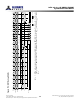
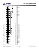
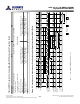
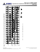
Table Of Contents
- DDR3L SDRAM
- Description
- State Diagram
- Functional Description
- Functional Block Diagrams
- Ball Assignments and Descriptions
- Package Dimensions
- Electrical Specifications
- Thermal Characteristics
- Electrical Specifications – I DD Specifications and Conditions
- Electrical Characteristics – 1.35V IDD Specifications
- Electrical Specifications – DC and AC
- ODT Characteristics
- Output Driver Impedance
- Output Characteristics and Operating Conditions
- Speed Bin Tables
- Electrical Characteristics and AC Operating Conditions
- Electrical Characteristics and AC Operating Conditions
- Command and Address Setup, Hold, and Derating
- Data Setup, Hold, and Derating
- Commands – Truth Tables
- Commands
- Input Clock Frequency Change
- Write Leveling
- Initialization
- Voltage Initialization / Change
- Mode Registers
- Mode Register 0 (MR0)
- Mode Register 1 (MR1)
- Mode Register 2 (MR2)
- Mode Register 3 (MR3)
- MODE REGISTER SET (MRS) Command
- ZQ CALIBRATION Operation
- ACTIVATE Operation
- READ Operation
- WRITE Operation
- PRECHARGE Operation
- SELF REFRESH Operation
- Extended Temperature Usage
- Power-Down Mode
- RESET Operation
- On-Die Termination (ODT)
- Dynamic ODT
- Synchronous ODT Mode
- Asynchronous ODT Mode
- Asynchronous to Synchronous ODT Mode Transition (Power-Down Exit)
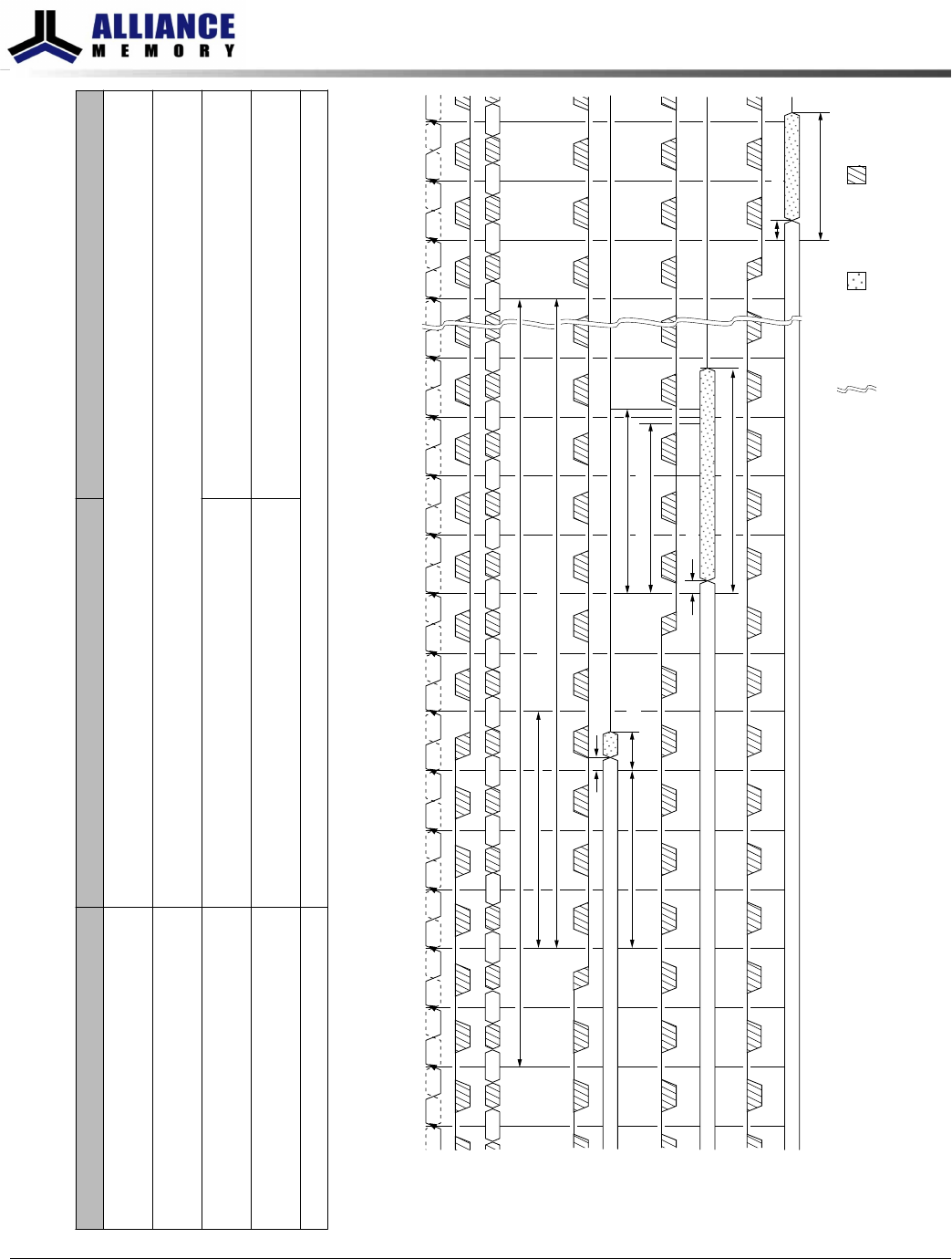
Table 89: ODT Parameters for Power-Down (DLL Off) Entry and Exit Transition Period
Description Min Max
Power-down entry transition period
(power-down entry)
Greater of:
t
ANPD or
t
RFC - refresh to CKE LOW
Power-down exit transition period
(power-down exit)
t
ANPD +
t
XPDLL
ODT to R
TT
turn-on delay
(ODTLon = WL - 2)
Lesser of:
t
AONPD (MIN) (2ns) or
ODTLon ×
t
CK +
t
AON (MIN)
Greater of:
t
AONPD (MAX) (8.5ns) or
ODTLon ×
t
CK +
t
AON (MAX)
ODT to R
TT
turn-off delay
(ODTLoff = WL - 2)
Lesser of:
t
AOFPD (MIN) (2ns) or
ODTLoff ×
t
CK +
t
AOF (MIN)
Greater of:
t
AOFPD (MAX) (8.5ns) or
ODTLoff ×
t
CK +
t
AOF (MAX)
t
ANPD WL - 1 (greater of ODTLoff + 1 or ODTLon + 1)
Figure 116: Synchronous to Asynchronous Transition During Precharge Power-Down (DLL Off) Entry
T0 T1 T2 T3 T4 T5 T6 T7 T8 T9
t
AOFPD (MAX)
ODTLoff
T10 T11 T12 T13 Ta0 Ta1 Ta3Ta2
CK
CK#
DRAM R
TT
B
asynchronous
or synchronous
R
TT,nom
DRAM R
TT
C
asynchronous
R
TT,nom
Don’t CareTransitioning
CKE
NOP NOP NOPNOP NOPCommand NOPREF NOP NOP NOP NOPNOP NOP NOP NOPNOP NOP NOP
PDE transition period
Indicates break
in time scale
ODTLoff +
t
AOFPD (MIN)
t
AOFPD (MAX)
t
AOFPD (MIN)
ODTLoff +
t
AOFPD (MAX)
t
AOFPD (MIN)
t
ANPD
t
AOF (MIN)
t
AOF (MAX)
DRAM R
TT
A
synchronous
R
TT,nom
ODT A
synchronous
ODT C
asynchronous
ODT B
asynchronous
or synchronous
t
RFC (MIN)
Note:
1. AL = 0; CWL = 5; ODTL(off) = WL - 2 = 3.
8Gb: x4, x8, x16 DDR3L SDRAM
Asynchronous ODT Mode
203
Rev.2.0 June 2016
© 2015 Alliance Memory, Inc. All rights reserved.
Alliance Memory Inc. reserves the right to change products or specification without notice
Alliance Memory Inc. 511 Taylor Way, San Carlos, CA 94070
TEL: (650) 610-6800 FAX: (650) 620-9211