
Datasheet
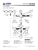
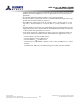
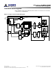
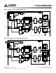
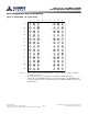
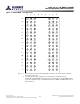
Table Of Contents
- DDR3L SDRAM
- Description
- State Diagram
- Functional Description
- Functional Block Diagrams
- Ball Assignments and Descriptions
- Package Dimensions
- Electrical Specifications
- Thermal Characteristics
- Electrical Specifications – I DD Specifications and Conditions
- Electrical Characteristics – 1.35V IDD Specifications
- Electrical Specifications – DC and AC
- ODT Characteristics
- Output Driver Impedance
- Output Characteristics and Operating Conditions
- Speed Bin Tables
- Electrical Characteristics and AC Operating Conditions
- Electrical Characteristics and AC Operating Conditions
- Command and Address Setup, Hold, and Derating
- Data Setup, Hold, and Derating
- Commands – Truth Tables
- Commands
- Input Clock Frequency Change
- Write Leveling
- Initialization
- Voltage Initialization / Change
- Mode Registers
- Mode Register 0 (MR0)
- Mode Register 1 (MR1)
- Mode Register 2 (MR2)
- Mode Register 3 (MR3)
- MODE REGISTER SET (MRS) Command
- ZQ CALIBRATION Operation
- ACTIVATE Operation
- READ Operation
- WRITE Operation
- PRECHARGE Operation
- SELF REFRESH Operation
- Extended Temperature Usage
- Power-Down Mode
- RESET Operation
- On-Die Termination (ODT)
- Dynamic ODT
- Synchronous ODT Mode
- Asynchronous ODT Mode
- Asynchronous to Synchronous ODT Mode Transition (Power-Down Exit)
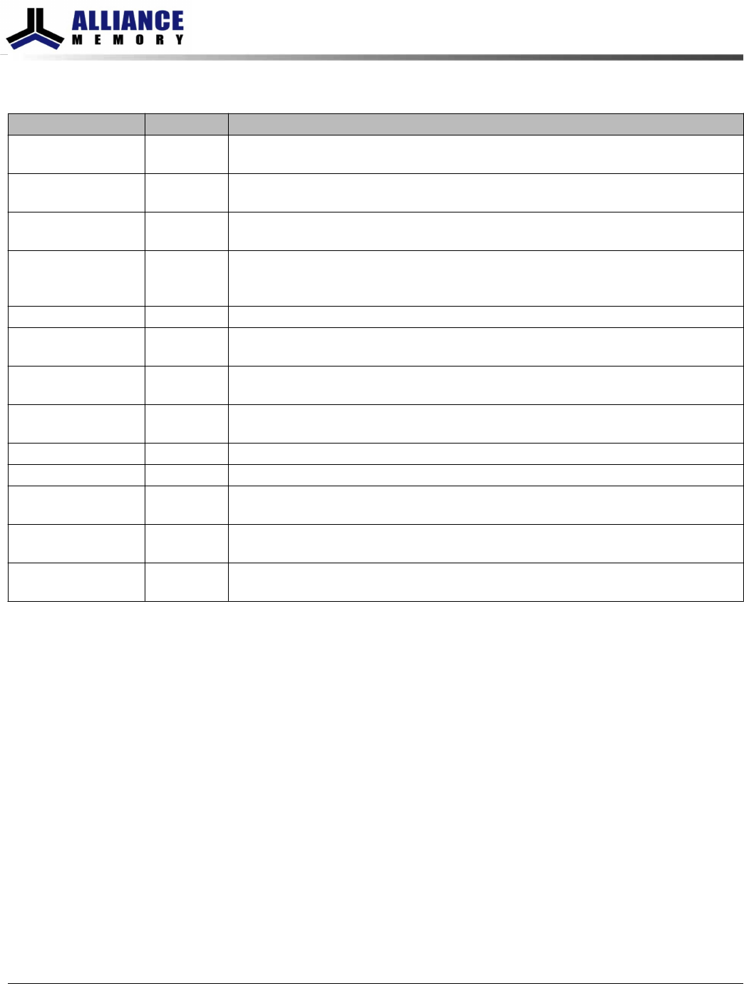
Table 3: 78-Ball FBGA – x4, x8 Ball Descriptions (Continued)
Symbol Type Description
DQ[3:0] I/O Data input/output: Bidirectional data bus for the x4 configuration. DQ[3:0] are
referenced to V
REFDQ
.
DQ[7:0] I/O Data input/output: Bidirectional data bus for the x8 configuration. DQ[7:0] are
referenced to V
REFDQ
.
DQS, DQS# I/O Data strobe: Output with read data. Edge-aligned with read data. Input with write
data. Center-aligned to write data.
TDQS, TDQS# Output Termination data strobe: Applies to the x8 configuration only. When TDQS is
enabled, DM is disabled, and the TDQS and TDQS# balls provide termination
resistance.
V
DD
Supply Power supply: 1.35V (1.283–1.45V) / 1.5V ±0.075V (backward compatible).
V
DDQ
Supply DQ power supply: 1.35V (1.283–1.45V) /1.5V ±0.075V (backward compatible). Isola-
ted on the device for improved noise immunity.
V
REFCA
Supply Reference voltage for control, command, and address: V
REFCA
must be
maintained at all times (including self refresh) for proper device operation.
V
REFDQ
Supply Reference voltage for data: V
REFDQ
must be maintained at all times (excluding self
refresh) for proper device operation.
V
SS
Supply Ground.
V
SSQ
Supply DQ ground: Isolated on the device for improved noise immunity.
ZQ Reference External reference ball for output drive calibration: This ball is tied to an
external 240Ω resistor (RZQ), which is tied to V
SSQ
.
NC – No connect: These balls should be left unconnected (the ball has no connection to
the DRAM or to other balls).
NF – No function: When configured as a x4 device, these balls are NF. When configured
as a x8 device, these balls are defined as TDQS#, DQ[7:4].
8Gb: x4, x8, x16 DDR3L SDRAM
Ball Assignments and Descriptions
19
Rev.2.0 June 2016
© 2015 Alliance Memory, Inc. All rights reserved.
Alliance Memory Inc. reserves the right to change products or specification without notice
Alliance Memory Inc. 511 Taylor Way, San Carlos, CA 94070
TEL: (650) 610-6800 FAX: (650) 620-9211