
Datasheet
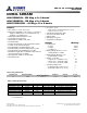
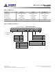
Table Of Contents
- DDR3L SDRAM
- Description
- State Diagram
- Functional Description
- Functional Block Diagrams
- Ball Assignments and Descriptions
- Package Dimensions
- Electrical Specifications
- Thermal Characteristics
- Electrical Specifications – I DD Specifications and Conditions
- Electrical Characteristics – 1.35V IDD Specifications
- Electrical Specifications – DC and AC
- ODT Characteristics
- Output Driver Impedance
- Output Characteristics and Operating Conditions
- Speed Bin Tables
- Electrical Characteristics and AC Operating Conditions
- Electrical Characteristics and AC Operating Conditions
- Command and Address Setup, Hold, and Derating
- Data Setup, Hold, and Derating
- Commands – Truth Tables
- Commands
- Input Clock Frequency Change
- Write Leveling
- Initialization
- Voltage Initialization / Change
- Mode Registers
- Mode Register 0 (MR0)
- Mode Register 1 (MR1)
- Mode Register 2 (MR2)
- Mode Register 3 (MR3)
- MODE REGISTER SET (MRS) Command
- ZQ CALIBRATION Operation
- ACTIVATE Operation
- READ Operation
- WRITE Operation
- PRECHARGE Operation
- SELF REFRESH Operation
- Extended Temperature Usage
- Power-Down Mode
- RESET Operation
- On-Die Termination (ODT)
- Dynamic ODT
- Synchronous ODT Mode
- Asynchronous ODT Mode
- Asynchronous to Synchronous ODT Mode Transition (Power-Down Exit)

DDR3L SDRAM
AS4C2GM4D3L– 256 Meg x 4 x 8 banks*
AS4C1G8MD3L– 128 Meg x 8 x 8 banks
AS4C512M16D3L – 64 Meg x 16 x 8 banks
Features
•V
DD
= V
DDQ
= 1.35V (1.283–1.45V)
• Backward compatible to V
DD
= V
DDQ
= 1.5V ±0.075V
– Supports DDR3L devices to be backward com-
patible in 1.5V applications
• Differential bidirectional data strobe
•8n-bit prefetch architecture
• Differential clock inputs (CK, CK#)
• 8 internal banks
• Nominal and dynamic on-die termination (ODT)
for data, strobe, and mask signals
• Programmable CAS (READ) latency (CL)
• Programmable posted CAS additive latency (AL)
• Programmable CAS (WRITE) latency (CWL)
• Fixed burst length (BL) of 8 and burst chop (BC) of 4
(via the mode register set [MRS])
• Selectable BC4 or BL8 on-the-fly (OTF)
• Self refresh mode
•T
C
of 0°C to +95°C
– 64ms, 8192-cycle refresh at 0°C to +85°C
– 32ms at +85°C to +95°C
• Self refresh temperature (SRT)
• Automatic self refresh (ASR)
• Write leveling
• Multipurpose register
• Output driver calibration
Options Marking
• Configuration
– 2 Gig x 4
2GM4
– 1 Gig x 8
1GM8
– 512 Meg x 16 512M16
• FBGA package (Pb-free) – x4, x8
– 78-ball (9mm x 13.2mm)
B
• FBGA package (Pb-free) – x16
– 96-ball (9mm x 14mm)
B
• Timing – cycle time
– 938ps @ CL = 14 (DDR3-2133)
– 1.07ns @ CL = 13 (DDR3-1866)
– 1.25ns @ CL = 11 (DDR3-1600)
• Operating temperature
– Commercial (0°C ≤ T
C
≤ +95°C)
– Industrial (–40°C ≤ T
C
≤ +95°C)
-09
-10
-12
C
Key Timing Parameters
Speed Grade Data Rate (MT/s)
Target
t
RCD-
t
RP-CL
t
RCD (ns)
t
RP (ns) CL (ns)
-12 1600 11-11-11 13.75 13.75 13.75
Notes: 1.
Alliance Memory Inc will only offer the -12 1.25ns @ CL = 11 (DDR3-1600) option
1
Rev 2.0 June 2016
© 2015 Alliance Memory, Inc. All rights reserved.
Alliance Memory Inc. reserves the right to change products or specification without notice
Alliance Memory Inc. 511 Taylor Way, San Carlos, CA 94070
TEL: (650) 610-6800 FAX: (650) 620-9211
Part Number
Power Supply
Package
AS4C2GM4D3L-12BCN
*
1600
1.35V (1.283–1.45V)
78-ball (9mm x 13.2mm) FBGA
AS4C2GM4D3L-12BIN*
1600
1.35V (1.283–1.45V)
78-ball (9mm x 13.2mm) FBGA
AS
4C1G8MD3L-12BCN
1600
1.35V (1.283–1.45V)
78-ball (9mm x 13.2mm) FBGA
AS
4C1G8MD3L-12BIN
1600
1.35V (1.283–1.45V)
78-ball (9mm x 13.2mm)!FBGA
AS4C512M16D3L-12BCN 1600
1.35V (1.283–1.45V)
96-ball (9mm x 14mm) FBGA
AS4C512M16D3L-12BIN 1600
1.35V (1.283–1.45V)
96-ball (9mm x 14mm) FBGA
Table 1:Ordering Information
800 MHz
800 MHz
800 MHz
800 MHz
800 MHz
800 MHz
2.*
not released yet
8Gb: x4, x8, x16 DDR3L SDRAM
Description
Clock Frequency Data Rate(MT/s)
I