
Datasheet

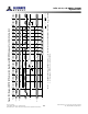
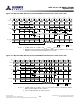
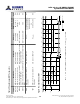
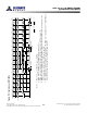
Table Of Contents
- DDR3L SDRAM
- Description
- State Diagram
- Functional Description
- Functional Block Diagrams
- Ball Assignments and Descriptions
- Package Dimensions
- Electrical Specifications
- Thermal Characteristics
- Electrical Specifications – I DD Specifications and Conditions
- Electrical Characteristics – 1.35V IDD Specifications
- Electrical Specifications – DC and AC
- ODT Characteristics
- Output Driver Impedance
- Output Characteristics and Operating Conditions
- Speed Bin Tables
- Electrical Characteristics and AC Operating Conditions
- Electrical Characteristics and AC Operating Conditions
- Command and Address Setup, Hold, and Derating
- Data Setup, Hold, and Derating
- Commands – Truth Tables
- Commands
- Input Clock Frequency Change
- Write Leveling
- Initialization
- Voltage Initialization / Change
- Mode Registers
- Mode Register 0 (MR0)
- Mode Register 1 (MR1)
- Mode Register 2 (MR2)
- Mode Register 3 (MR3)
- MODE REGISTER SET (MRS) Command
- ZQ CALIBRATION Operation
- ACTIVATE Operation
- READ Operation
- WRITE Operation
- PRECHARGE Operation
- SELF REFRESH Operation
- Extended Temperature Usage
- Power-Down Mode
- RESET Operation
- On-Die Termination (ODT)
- Dynamic ODT
- Synchronous ODT Mode
- Asynchronous ODT Mode
- Asynchronous to Synchronous ODT Mode Transition (Power-Down Exit)
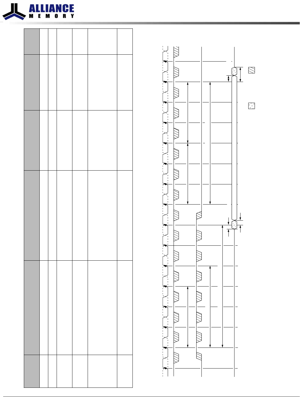
Table 87: Synchronous ODT Parameters
Symbol Description Begins at Defined to
Definition for All
DDR3L Speed Bins
Unit
ODTLon ODT synchronous turn-on delay ODT registered HIGH R
TT(ON)
±
t
AON CWL + AL - 2
t
CK
ODTLoff ODT synchronous turn-off delay ODT registered HIGH R
TT(OFF)
±
t
AOF CWL +AL - 2
t
CK
ODTH4 ODT minimum HIGH time after ODT
assertion or WRITE (BC4)
ODT registered HIGH or write regis-
tration with ODT HIGH
ODT registered LOW 4
t
CK
t
CK
ODTH8 ODT minimum HIGH time after WRITE
(BL8)
Write registration with ODT HIGH ODT registered LOW 6
t
CK
t
CK
t
AON ODT turn-on relative to ODTLon
completion
Completion of ODTLon R
TT(ON)
See Electrical Charac-
teristics and AC Oper-
ating Conditions ta-
ble
ps
t
AOF ODT turn-off relative to ODTLoff
completion
Completion of ODTLoff R
TT(OFF)
0.5
t
CK ± 0.2
t
CK
t
CK
Figure 112: Synchronous ODT
T0 T1 T2 T3 T4 T5 T6 T7 T8 T9
CWL - 2AL = 3AL = 3
t
AON (MAX)
t
AOF (MAX)
T10 T11 T12 T13 T14 T15
CK
CK#
R
TT
ODT
Don’t CareTransitioning
R
TT,nom
CKE
t
AOF (MIN)
ODTLoff = CWL + AL - 2
ODTLon = CWL + AL - 2
ODTH4 (MIN)
t
AON (MIN)
Note:
1. AL = 3; CWL = 5; ODTLon = WL = 6.0; ODTLoff = WL - 2 = 6. R
TT,nom
is enabled.
8Gb: x4, x8, x16 DDR3L SDRAM
Synchronous ODT Mode
196
Rev.2.0 June 2016
© 2015 Alliance Memory, Inc. All rights reserved.
Alliance Memory Inc. reserves the right to change products or specification without notice
Alliance Memory Inc. 511 Taylor Way, San Carlos, CA 94070
TEL: (650) 610-6800 FAX: (650) 620-9211