
Datasheet

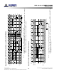
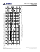
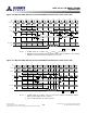
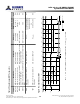
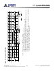
Table Of Contents
- DDR3L SDRAM
- Description
- State Diagram
- Functional Description
- Functional Block Diagrams
- Ball Assignments and Descriptions
- Package Dimensions
- Electrical Specifications
- Thermal Characteristics
- Electrical Specifications – I DD Specifications and Conditions
- Electrical Characteristics – 1.35V IDD Specifications
- Electrical Specifications – DC and AC
- ODT Characteristics
- Output Driver Impedance
- Output Characteristics and Operating Conditions
- Speed Bin Tables
- Electrical Characteristics and AC Operating Conditions
- Electrical Characteristics and AC Operating Conditions
- Command and Address Setup, Hold, and Derating
- Data Setup, Hold, and Derating
- Commands – Truth Tables
- Commands
- Input Clock Frequency Change
- Write Leveling
- Initialization
- Voltage Initialization / Change
- Mode Registers
- Mode Register 0 (MR0)
- Mode Register 1 (MR1)
- Mode Register 2 (MR2)
- Mode Register 3 (MR3)
- MODE REGISTER SET (MRS) Command
- ZQ CALIBRATION Operation
- ACTIVATE Operation
- READ Operation
- WRITE Operation
- PRECHARGE Operation
- SELF REFRESH Operation
- Extended Temperature Usage
- Power-Down Mode
- RESET Operation
- On-Die Termination (ODT)
- Dynamic ODT
- Synchronous ODT Mode
- Asynchronous ODT Mode
- Asynchronous to Synchronous ODT Mode Transition (Power-Down Exit)

Synchronous ODT Mode
Synchronous ODT mode is selected whenever the DLL is turned on and locked and
when either R
TT,nom
or R
TT(WR)
is enabled. Based on the power-down definition, these
modes are:
• Any bank active with CKE HIGH
• Refresh mode with CKE HIGH
• Idle mode with CKE HIGH
• Active power-down mode (regardless of MR0[12])
• Precharge power-down mode if DLL is enabled by MR0[12] during precharge power-
down
ODT Latency and Posted ODT
In synchronous ODT mode, R
TT
turns on ODTLon clock cycles after ODT is sampled
HIGH by a rising clock edge and turns off ODTLoff clock cycles after ODT is registered
LOW by a rising clock edge. The actual on/off times varies by
t
AON and
t
AOF around
each clock edge (see Table 87 (page 196)). The ODT latency is tied to the WRITE latency
(WL) by ODTLon = WL - 2 and ODTLoff = WL - 2.
Since write latency is made up of CAS WRITE latency (CWL) and additive latency (AL),
the AL programmed into the mode register (MR1[4, 3]) also applies to the ODT signal.
The device’s internal ODT signal is delayed a number of clock cycles defined by the AL
relative to the external ODT signal. Thus, ODTLon = CWL + AL - 2 and ODTLoff = CWL +
AL - 2.
Timing Parameters
Synchronous ODT mode uses the following timing parameters: ODTLon, ODTLoff,
ODTH4, ODTH8,
t
AON, and
t
AOF. The minimum R
TT
turn-on time (
t
AON [MIN]) is the
point at which the device leaves High-Z and ODT resistance begins to turn on. Maxi-
mum R
TT
turn-on time (
t
AON [MAX]) is the point at which ODT resistance is fully on.
Both are measured relative to ODTLon. The minimum R
TT
turn-off time (
t
AOF [MIN]) is
the point at which the device starts to turn off ODT resistance. The maximum R
TT
turn
off time (
t
AOF [MAX]) is the point at which ODT has reached High-Z. Both are measured
from ODTLoff.
When ODT is asserted, it must remain HIGH until ODTH4 is satisfied. If a WRITE com-
mand is registered by the DRAM with ODT HIGH, then ODT must remain HIGH until
ODTH4 (BC4) or ODTH8 (BL8) after the WRITE command (see Figure 113 (page 197)).
ODTH4 and ODTH8 are measured from ODT registered HIGH to ODT registered LOW
or from the registration of a WRITE command until ODT is registered LOW.
8Gb: x4, x8, x16 DDR3L SDRAM
Synchronous ODT Mode
195
Rev.2.0 June 2016
© 2015 Alliance Memory, Inc. All rights reserved.
Alliance Memory Inc. reserves the right to change products or specification without notice
Alliance Memory Inc. 511 Taylor Way, San Carlos, CA 94070
TEL: (650) 610-6800 FAX: (650) 620-9211