
Datasheet
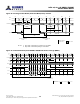
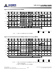


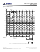
Table Of Contents
- DDR3L SDRAM
- Description
- State Diagram
- Functional Description
- Functional Block Diagrams
- Ball Assignments and Descriptions
- Package Dimensions
- Electrical Specifications
- Thermal Characteristics
- Electrical Specifications – I DD Specifications and Conditions
- Electrical Characteristics – 1.35V IDD Specifications
- Electrical Specifications – DC and AC
- ODT Characteristics
- Output Driver Impedance
- Output Characteristics and Operating Conditions
- Speed Bin Tables
- Electrical Characteristics and AC Operating Conditions
- Electrical Characteristics and AC Operating Conditions
- Command and Address Setup, Hold, and Derating
- Data Setup, Hold, and Derating
- Commands – Truth Tables
- Commands
- Input Clock Frequency Change
- Write Leveling
- Initialization
- Voltage Initialization / Change
- Mode Registers
- Mode Register 0 (MR0)
- Mode Register 1 (MR1)
- Mode Register 2 (MR2)
- Mode Register 3 (MR3)
- MODE REGISTER SET (MRS) Command
- ZQ CALIBRATION Operation
- ACTIVATE Operation
- READ Operation
- WRITE Operation
- PRECHARGE Operation
- SELF REFRESH Operation
- Extended Temperature Usage
- Power-Down Mode
- RESET Operation
- On-Die Termination (ODT)
- Dynamic ODT
- Synchronous ODT Mode
- Asynchronous ODT Mode
- Asynchronous to Synchronous ODT Mode Transition (Power-Down Exit)
Table 80: Truth Table – ODT (Nominal)
Note 1 applies to the entire table
MR1[9, 6, 2] ODT Pin DRAM Termination State DRAM State Notes
000 0 R
TT,nom
disabled, ODT off Any valid 2
000 1 R
TT,nom
disabled, ODT on Any valid except self refresh, read 3
000–101 0 R
TT,nom
enabled, ODT off Any valid 2
000–101 1 R
TT,nom
enabled, ODT on Any valid except self refresh, read 3
110 and 111 X R
TT,nom
reserved, ODT on or off Illegal
Notes:
1. Assumes dynamic ODT is disabled (see Dynamic ODT (page 189) when enabled).
2. ODT is enabled and active during most writes for proper termination, but it is not illegal
for it to be off during writes.
3. ODT must be disabled during reads. The R
TT,nom
value is restricted during writes. Dynam-
ic ODT is applicable if enabled.
Nominal ODT resistance R
TT,nom
is defined by MR1[9, 6, 2], as shown in Mode Register 1
(MR1) Definition. The R
TT,nom
termination value applies to the output pins previously
mentioned. DDR3 SDRAM supports multiple R
TT,nom
values based on RZQ/n where n
can be 2, 4, 6, 8, or 12 and RZQ is 240Ω. R
TT,nom
termination is allowed any time after the
DRAM is initialized, calibrated, and not performing read access, or when it is not in self
refresh mode.
Write accesses use R
TT,nom
if dynamic ODT (R
TT(WR)
) is disabled. If R
TT,nom
is used dur-
ing writes, only RZQ/2, RZQ/4, and RZQ/6 are allowed (see Table 84 (page 190)). ODT
timings are summarized in Table 81 (page 188), as well as listed in the Electrical Char-
acteristics and AC Operating Conditions table.
Examples of nominal ODT timing are shown in conjunction with the synchronous
mode of operation in Synchronous ODT Mode (page 195).
Table 81: ODT Parameters
Symbol Description Begins at Defined to
Definition for All
DDR3L Speed Bins
Unit
ODTLon ODT synchronous turn-on delay ODT registered HIGH R
TT(ON)
±
t
AON CWL + AL - 2
t
CK
ODTLoff ODT synchronous turn-off delay ODT registered HIGH R
TT(OFF)
±
t
AOF CWL + AL - 2
t
CK
t
AONPD ODT asynchronous turn-on delay ODT registered HIGH R
TT(ON)
2–8.5 ns
t
AOFPD ODT asynchronous turn-off delay ODT registered HIGH R
TT(OFF)
2–8.5 ns
ODTH4 ODT minimum HIGH time after ODT
assertion or write (BC4)
ODT registered HIGH
or write registration
with ODT HIGH
ODT registered
LOW
4
t
CK
t
CK
ODTH8 ODT minimum HIGH time after
write (BL8)
Write registration
with ODT HIGH
ODT registered
LOW
6
t
CK
t
CK
t
AON ODT turn-on relative to ODTLon
completion
Completion of
ODTLon
R
TT(ON)
See Electrical Charac-
teristics and AC Oper-
ating Conditions table
ps
t
AOF ODT turn-off relative to ODTLoff
completion
Completion of
ODTLoff
R
TT(OFF)
0.5
t
CK ± 0.2
t
CK
t
CK
8Gb: x4, x8, x16 DDR3L SDRAM
On-Die Termination (ODT)
188
Rev.2.0 June 2016
© 2015 Alliance Memory, Inc. All rights reserved.
Alliance Memory Inc. reserves the right to change products or specification without notice
Alliance Memory Inc. 511 Taylor Way, San Carlos, CA 94070
TEL: (650) 610-6800 FAX: (650) 620-9211