
Datasheet
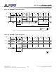


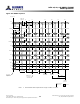
Table Of Contents
- DDR3L SDRAM
- Description
- State Diagram
- Functional Description
- Functional Block Diagrams
- Ball Assignments and Descriptions
- Package Dimensions
- Electrical Specifications
- Thermal Characteristics
- Electrical Specifications – I DD Specifications and Conditions
- Electrical Characteristics – 1.35V IDD Specifications
- Electrical Specifications – DC and AC
- ODT Characteristics
- Output Driver Impedance
- Output Characteristics and Operating Conditions
- Speed Bin Tables
- Electrical Characteristics and AC Operating Conditions
- Electrical Characteristics and AC Operating Conditions
- Command and Address Setup, Hold, and Derating
- Data Setup, Hold, and Derating
- Commands – Truth Tables
- Commands
- Input Clock Frequency Change
- Write Leveling
- Initialization
- Voltage Initialization / Change
- Mode Registers
- Mode Register 0 (MR0)
- Mode Register 1 (MR1)
- Mode Register 2 (MR2)
- Mode Register 3 (MR3)
- MODE REGISTER SET (MRS) Command
- ZQ CALIBRATION Operation
- ACTIVATE Operation
- READ Operation
- WRITE Operation
- PRECHARGE Operation
- SELF REFRESH Operation
- Extended Temperature Usage
- Power-Down Mode
- RESET Operation
- On-Die Termination (ODT)
- Dynamic ODT
- Synchronous ODT Mode
- Asynchronous ODT Mode
- Asynchronous to Synchronous ODT Mode Transition (Power-Down Exit)
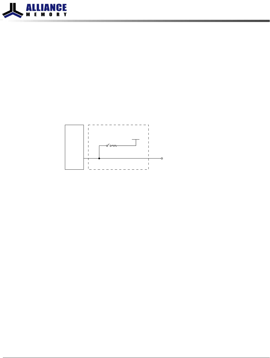
On-Die Termination (ODT)
On-die termination (ODT) is a feature that enables the DRAM to enable/disable and
turn on/off termination resistance for each DQ, DQS, DQS#, and DM for the x4 and x8
configurations (and TDQS, TDQS# for the x8 configuration, when enabled). ODT is ap-
plied to each DQ, UDQS, UDQS#, LDQS, LDQS#, UDM, and LDM signal for the x16 con-
figuration.
ODT is designed to improve signal integrity of the memory channel by enabling the
DRAM controller to independently turn on/off the DRAM’s internal termination resist-
ance for any grouping of DRAM devices. ODT is not supported during DLL disable
mode (simple functional representation shown below). The switch is enabled by the in-
ternal ODT control logic, which uses the external ODT ball and other control informa-
tion.
Figure 106: On-Die Termination
ODT
V
DDQ
/2
R
TT
Switch
DQ, DQS, DQS#,
DM, TDQS, TDQS#
To other
circuitry
such as
RCV,
. . .
Functional Representation of ODT
The value of R
TT
(ODT termination resistance value) is determined by the settings of
several mode register bits (see Table 85 (page 191)). The ODT ball is ignored while in
self refresh mode (must be turned off prior to self refresh entry) or if mode registers
MR1 and MR2 are programmed to disable ODT. ODT is comprised of nominal ODT and
dynamic ODT modes and either of these can function in synchronous or asynchronous
mode (when the DLL is off during precharge power-down or when the DLL is synchro-
nizing). Nominal ODT is the base termination and is used in any allowable ODT state.
Dynamic ODT is applied only during writes and provides OTF switching from no R
TT
or
R
TT,nom
to R
TT(WR)
.
The actual effective termination, R
TT(EFF)
, may be different from R
TT
targeted due to
nonlinearity of the termination. For R
TT(EFF)
values and calculations, see Table 30
(page 51).
Nominal ODT
ODT (NOM) is the base termination resistance for each applicable ball; it is enabled or
disabled via MR1[9, 6, 2] (see Mode Register 1 (MR1) Definition), and it is turned on or
off via the ODT ball.
8Gb: x4, x8, x16 DDR3L SDRAM
On-Die Termination (ODT)
187
Rev.2.0 June 2016
© 2015 Alliance Memory, Inc. All rights reserved.
Alliance Memory Inc. reserves the right to change products or specification without notice
Alliance Memory Inc. 511 Taylor Way, San Carlos, CA 94070
TEL: (650) 610-6800 FAX: (650) 620-9211