
Datasheet
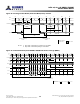
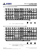


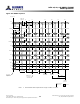
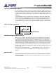
Table Of Contents
- DDR3L SDRAM
- Description
- State Diagram
- Functional Description
- Functional Block Diagrams
- Ball Assignments and Descriptions
- Package Dimensions
- Electrical Specifications
- Thermal Characteristics
- Electrical Specifications – I DD Specifications and Conditions
- Electrical Characteristics – 1.35V IDD Specifications
- Electrical Specifications – DC and AC
- ODT Characteristics
- Output Driver Impedance
- Output Characteristics and Operating Conditions
- Speed Bin Tables
- Electrical Characteristics and AC Operating Conditions
- Electrical Characteristics and AC Operating Conditions
- Command and Address Setup, Hold, and Derating
- Data Setup, Hold, and Derating
- Commands – Truth Tables
- Commands
- Input Clock Frequency Change
- Write Leveling
- Initialization
- Voltage Initialization / Change
- Mode Registers
- Mode Register 0 (MR0)
- Mode Register 1 (MR1)
- Mode Register 2 (MR2)
- Mode Register 3 (MR3)
- MODE REGISTER SET (MRS) Command
- ZQ CALIBRATION Operation
- ACTIVATE Operation
- READ Operation
- WRITE Operation
- PRECHARGE Operation
- SELF REFRESH Operation
- Extended Temperature Usage
- Power-Down Mode
- RESET Operation
- On-Die Termination (ODT)
- Dynamic ODT
- Synchronous ODT Mode
- Asynchronous ODT Mode
- Asynchronous to Synchronous ODT Mode Transition (Power-Down Exit)
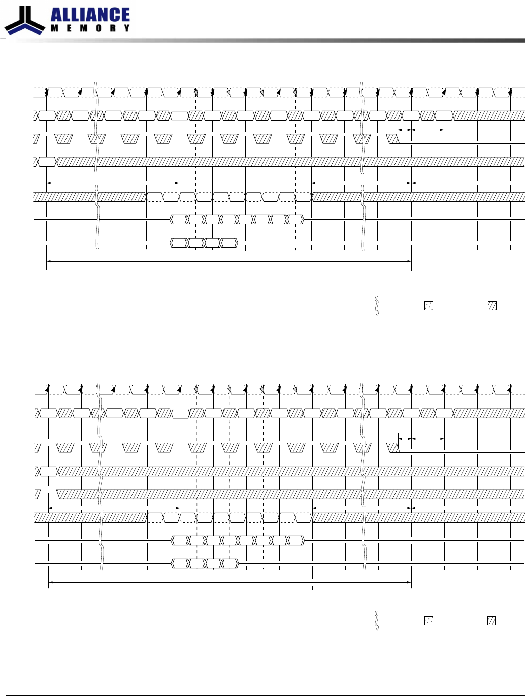
Figure 98: Power-Down Entry After WRITE
T0 T1 Ta0 Ta1 Ta2 Ta3 Ta4 Ta5 Ta6 Ta7 Tb0 Tb1 Tb2 Tb3 Tb4
NOPWRITE
Valid
NOP NOP NOP NOP NOP NOP NOP NOP NOP NOP NOP
CK
CK#
Command
DQ BL8
DQ BC4
DQS, DQS#
Address
CKE
t
CPDED
Power-down or
self refresh entry
1
Don’t CareTransitioning Data
t
WRPDEN
DI
n + 3
DI
n + 1
DI
n + 2
DI
n
t
PD
Indicates break
in time scale
DI
n + 3
DI
n + 2
DI
n + 1
DI
n
DI
n + 6
DI
n + 7
DI
n + 5
DI
n + 4
t
IS
WL = AL + CWL
t
WR
Note:
1. CKE can go LOW 2
t
CK earlier if BC4MRS.
Figure 99: Power-Down Entry After WRITE with Auto Precharge (WRAP)
T0 T1 Ta0 Ta1 Ta2 Ta3 Ta4 Ta5 Ta6 Ta7 Tb0 Tb1
Don’t CareTransitioning Data
Tb2 Tb3 Tb4
NOPWRAP
Valid
NOP NOP NOP NOP NOP NOP NOP NOP NOP NOP NOP
CK
CK#
Command
DQ BL8
DQ BC4
DQS, DQS#
Address
A10
CKE
t
PD
t
WRAPDEN
Power-down or
self refresh entry
2
Start internal
precharge
t
CPDED
t
IS
Indicates break
in time scale
DI
n + 3
DI
n + 2
DI
n + 1
DI
n
DI
n + 6
DI
n + 7
DI
n + 5
DI
n + 4
DI
n + 3
DI
n + 2
DI
n + 1
DI
n
WR
1
WL = AL + CWL
Notes:
1.
t
WR is programmed through MR0[11:9] and represents
t
WRmin (ns)/
t
CK rounded up to
the next integer
t
CK.
2. CKE can go LOW 2
t
CK earlier if BC4MRS.
8Gb: x4, x8, x16 DDR3L SDRAM
Power-Down Mode
181
Rev.2.0 June 2016
© 2015 Alliance Memory, Inc. All rights reserved.
Alliance Memory Inc. reserves the right to change products or specification without notice
Alliance Memory Inc. 511 Taylor Way, San Carlos, CA 94070
TEL: (650) 610-6800 FAX: (650) 620-9211