
Datasheet
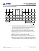

Table Of Contents
- DDR3L SDRAM
- Description
- State Diagram
- Functional Description
- Functional Block Diagrams
- Ball Assignments and Descriptions
- Package Dimensions
- Electrical Specifications
- Thermal Characteristics
- Electrical Specifications – I DD Specifications and Conditions
- Electrical Characteristics – 1.35V IDD Specifications
- Electrical Specifications – DC and AC
- ODT Characteristics
- Output Driver Impedance
- Output Characteristics and Operating Conditions
- Speed Bin Tables
- Electrical Characteristics and AC Operating Conditions
- Electrical Characteristics and AC Operating Conditions
- Command and Address Setup, Hold, and Derating
- Data Setup, Hold, and Derating
- Commands – Truth Tables
- Commands
- Input Clock Frequency Change
- Write Leveling
- Initialization
- Voltage Initialization / Change
- Mode Registers
- Mode Register 0 (MR0)
- Mode Register 1 (MR1)
- Mode Register 2 (MR2)
- Mode Register 3 (MR3)
- MODE REGISTER SET (MRS) Command
- ZQ CALIBRATION Operation
- ACTIVATE Operation
- READ Operation
- WRITE Operation
- PRECHARGE Operation
- SELF REFRESH Operation
- Extended Temperature Usage
- Power-Down Mode
- RESET Operation
- On-Die Termination (ODT)
- Dynamic ODT
- Synchronous ODT Mode
- Asynchronous ODT Mode
- Asynchronous to Synchronous ODT Mode Transition (Power-Down Exit)
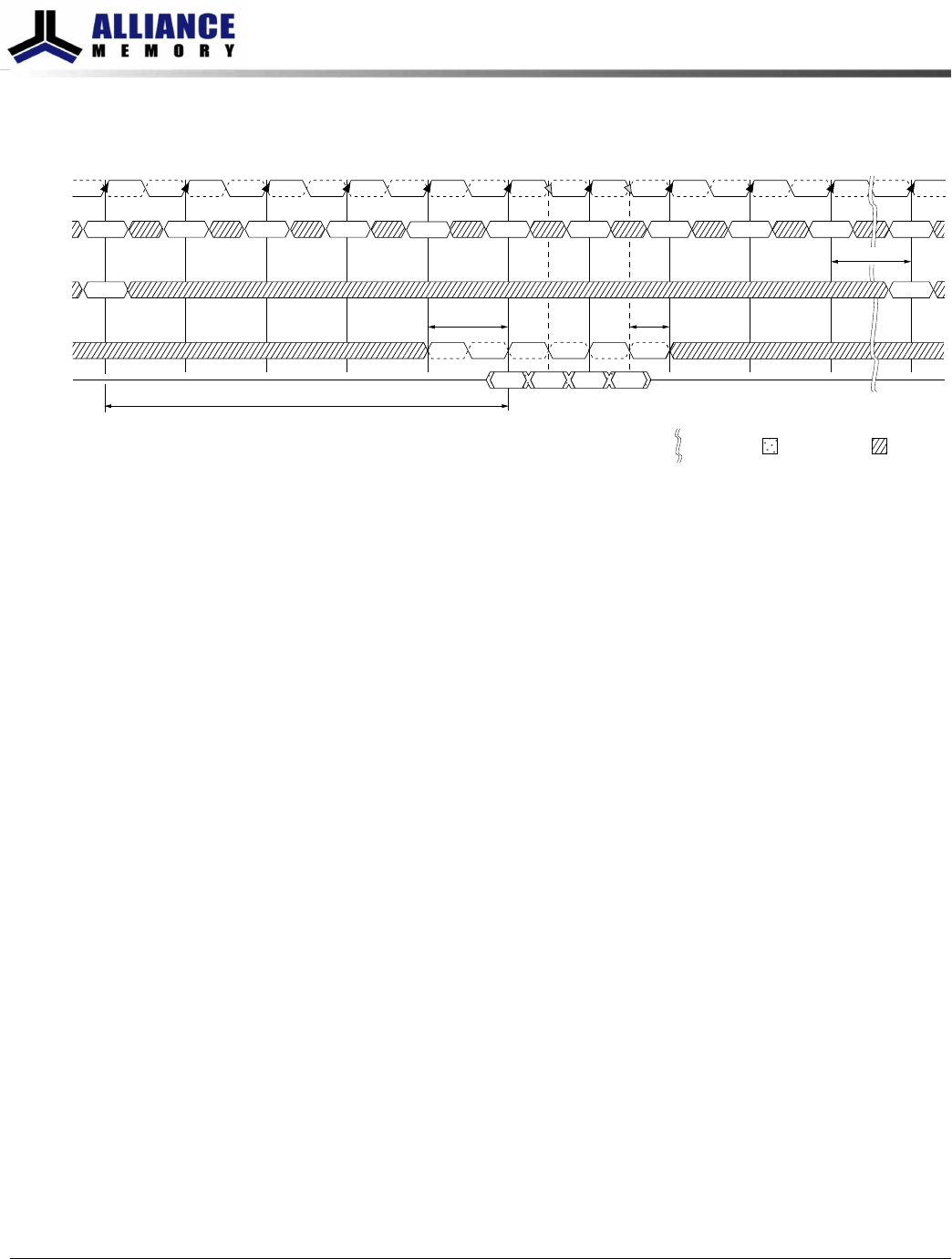
Figure 91: WRITE (BC4 OTF) to PRECHARGE
WL = 5
T0 T1 T2 T3 T4 T5 T6 T7 T8 T9 Tn
Don’t CareTransitioning Data
Bank,
Col n
NOPWRITE PRENOP NOP NOP NOP NOP NOP NOPNOP
CK
CK#
Command
1
DQ
4
DQS, DQS#
Address
3
t
WPST
t
WPRE
Indicates break
in time scale
DI
n + 3
DI
n + 2
DI
n + 1
DI
n
t
WR
2
Valid
Notes:
1. NOP commands are shown for ease of illustration; other commands may be valid at
these times.
2. The write recovery time (
t
WR) is referenced from the rising clock edge at T9.
t
WR speci-
fies the last burst WRITE cycle until the PRECHARGE command can be issued to the same
bank.
3. The BC4 setting is activated by MR0[1:0] = 01 and A12 = 0 during the WRITE command
at T0.
4. DI n = data-in for column n.
5. BC4 (OTF), WL = 5, RL = 5.
DQ Input Timing
Figure 82 (page 166) shows the strobe-to-clock timing during a WRITE burst. DQS,
DQS# must transition within 0.25
t
CK of the clock transitions, as limited by
t
DQSS. All
data and data mask setup and hold timings are measured relative to the DQS, DQS#
crossing, not the clock crossing.
The WRITE preamble and postamble are also shown in Figure 82 (page 166). One clock
prior to data input to the DRAM, DQS must be HIGH and DQS# must be LOW. Then for
a half clock, DQS is driven LOW (DQS# is driven HIGH) during the WRITE preamble,
t
WPRE. Likewise, DQS must be kept LOW by the controller after the last data is written
to the DRAM during the WRITE postamble,
t
WPST.
Data setup and hold times are also shown in Figure 82 (page 166). All setup and hold
times are measured from the crossing points of DQS and DQS#. These setup and hold
values pertain to data input and data mask input.
Additionally, the half period of the data input strobe is specified by
t
DQSH and
t
DQSL.
8Gb: x4, x8, x16 DDR3L SDRAM
WRITE Operation
172
Rev.2.0 June 2016
© 2015 Alliance Memory, Inc. All rights reserved.
Alliance Memory Inc. reserves the right to change products or specification without notice
Alliance Memory Inc. 511 Taylor Way, San Carlos, CA 94070
TEL: (650) 610-6800 FAX: (650) 620-9211