
Datasheet
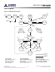
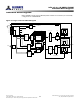
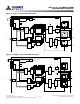
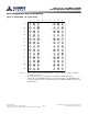
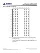
Table Of Contents
- DDR3L SDRAM
- Description
- State Diagram
- Functional Description
- Functional Block Diagrams
- Ball Assignments and Descriptions
- Package Dimensions
- Electrical Specifications
- Thermal Characteristics
- Electrical Specifications – I DD Specifications and Conditions
- Electrical Characteristics – 1.35V IDD Specifications
- Electrical Specifications – DC and AC
- ODT Characteristics
- Output Driver Impedance
- Output Characteristics and Operating Conditions
- Speed Bin Tables
- Electrical Characteristics and AC Operating Conditions
- Electrical Characteristics and AC Operating Conditions
- Command and Address Setup, Hold, and Derating
- Data Setup, Hold, and Derating
- Commands – Truth Tables
- Commands
- Input Clock Frequency Change
- Write Leveling
- Initialization
- Voltage Initialization / Change
- Mode Registers
- Mode Register 0 (MR0)
- Mode Register 1 (MR1)
- Mode Register 2 (MR2)
- Mode Register 3 (MR3)
- MODE REGISTER SET (MRS) Command
- ZQ CALIBRATION Operation
- ACTIVATE Operation
- READ Operation
- WRITE Operation
- PRECHARGE Operation
- SELF REFRESH Operation
- Extended Temperature Usage
- Power-Down Mode
- RESET Operation
- On-Die Termination (ODT)
- Dynamic ODT
- Synchronous ODT Mode
- Asynchronous ODT Mode
- Asynchronous to Synchronous ODT Mode Transition (Power-Down Exit)
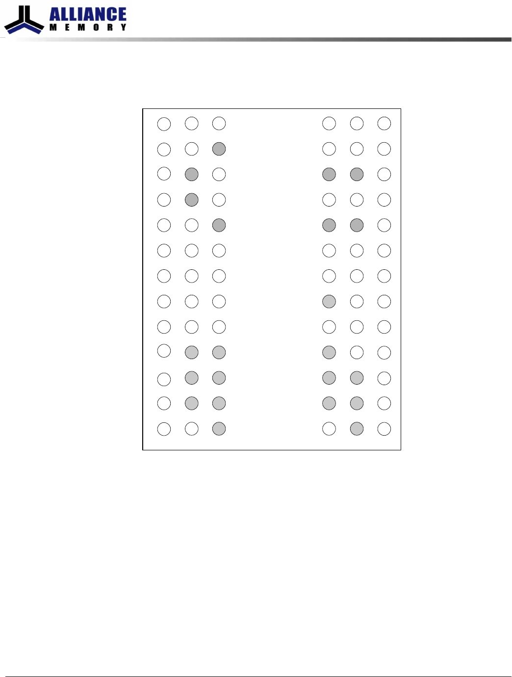
Ball Assignments and Descriptions
Figure 6: 78-Ball FBGA – x4, x8 (Top View)
1234 67895
V
SS
V
SS
V
DDQ
V
SSQ
V
REFDQ
NC
ODT
NC
V
SS
V
DD
V
SS
V
DD
V
SS
V
DD
V
SSQ
DQ2
NF, DQ6
V
DDQ
V
SS
V
DD
CS#
BA0
A3
A5
A7
RESET#
NC
DQ0
DQS
DQS#
NF, DQ4
RAS#
CAS#
WE#
BA2
A0
A2
A9
A13
NF, NF/TDQS#
DM, DM/TDQS
DQ1
V
DD
NF, DQ7
CK
CK#
A10/AP
A15
A12/BC#
A1
A11
A14
V
DD
V
DDQ
V
SSQ
V
SSQ
V
DDQ
NC
CKE
NC
V
SS
V
DD
V
SS
V
DD
V
SS
V
SS
V
SSQ
DQ3
V
SS
NF, DQ5
V
SS
V
DD
ZQ
V
REFCA
BA1
A4
A6
A8
A
B
C
D
E
F
G
H
J
K
L
M
N
Notes:
1. Ball descriptions listed in Table 3 (page 18) are listed as “x4, x8” if unique; otherwise,
x4 and x8 are the same.
2. A comma separates the configuration; a slash defines a selectable function.
Example D7 = NF, NF/TDQS#. NF applies to the x4 configuration only. NF/TDQS# applies
to the x8 configuration only—selectable between NF or TDQS# via MRS (symbols are de-
fined in Table 3).
8Gb: x4, x8, x16 DDR3L SDRAM
Ball Assignments and Descriptions
16
Rev.2.0 June 2016
© 2015 Alliance Memory, Inc. All rights reserved.
Alliance Memory Inc. reserves the right to change products or specification without notice
Alliance Memory Inc. 511 Taylor Way, San Carlos, CA 94070
TEL: (650) 610-6800 FAX: (650) 620-9211