
Datasheet
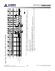

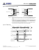
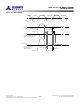
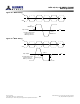
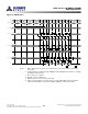
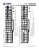

Table Of Contents
- DDR3L SDRAM
- Description
- State Diagram
- Functional Description
- Functional Block Diagrams
- Ball Assignments and Descriptions
- Package Dimensions
- Electrical Specifications
- Thermal Characteristics
- Electrical Specifications – I DD Specifications and Conditions
- Electrical Characteristics – 1.35V IDD Specifications
- Electrical Specifications – DC and AC
- ODT Characteristics
- Output Driver Impedance
- Output Characteristics and Operating Conditions
- Speed Bin Tables
- Electrical Characteristics and AC Operating Conditions
- Electrical Characteristics and AC Operating Conditions
- Command and Address Setup, Hold, and Derating
- Data Setup, Hold, and Derating
- Commands – Truth Tables
- Commands
- Input Clock Frequency Change
- Write Leveling
- Initialization
- Voltage Initialization / Change
- Mode Registers
- Mode Register 0 (MR0)
- Mode Register 1 (MR1)
- Mode Register 2 (MR2)
- Mode Register 3 (MR3)
- MODE REGISTER SET (MRS) Command
- ZQ CALIBRATION Operation
- ACTIVATE Operation
- READ Operation
- WRITE Operation
- PRECHARGE Operation
- SELF REFRESH Operation
- Extended Temperature Usage
- Power-Down Mode
- RESET Operation
- On-Die Termination (ODT)
- Dynamic ODT
- Synchronous ODT Mode
- Asynchronous ODT Mode
- Asynchronous to Synchronous ODT Mode Transition (Power-Down Exit)

WRITE Operation
WRITE bursts are initiated with a WRITE command. The starting column and bank ad-
dresses are provided with the WRITE command, and auto precharge is either enabled or
disabled for that access. If auto precharge is selected, the row being accessed is pre-
charged at the end of the WRITE burst. If auto precharge is not selected, the row will
remain open for subsequent accesses. After a WRITE command has been issued, the
WRITE burst may not be interrupted. For the generic WRITE commands used in Fig-
ure 82 (page 166) through Figure 90 (page 171), auto precharge is disabled.
During WRITE bursts, the first valid data-in element is registered on a rising edge of
DQS following the WRITE latency (WL) clocks later and subsequent data elements will
be registered on successive edges of DQS. WRITE latency (WL) is defined as the sum of
posted CAS additive latency (AL) and CAS WRITE latency (CWL): WL = AL + CWL. The
values of AL and CWL are programmed in the MR0 and MR2 registers, respectively. Prior
to the first valid DQS edge, a full cycle is needed (including a dummy crossover of DQS,
DQS#) and specified as the WRITE preamble shown in Figure 82 (page 166). The half
cycle on DQS following the last data-in element is known as the WRITE postamble.
The time between the WRITE command and the first valid edge of DQS is WL clocks
±
t
DQSS. Figure 83 (page 167) through Figure 90 (page 171) show the nominal case
where
t
DQSS = 0ns; however, Figure 82 (page 166) includes
t
DQSS (MIN) and
t
DQSS
(MAX) cases.
Data may be masked from completing a WRITE using data mask. The data mask occurs
on the DM ball aligned to the WRITE data. If DM is LOW, the WRITE completes normal-
ly. If DM is HIGH, that bit of data is masked.
Upon completion of a burst, assuming no other commands have been initiated, the DQ
will remain High-Z, and any additional input data will be ignored.
Data for any WRITE burst may be concatenated with a subsequent WRITE command to
provide a continuous flow of input data. The new WRITE command can be
t
CCD clocks
following the previous WRITE command. The first data element from the new burst is
applied after the last element of a completed burst. Figure 83 (page 167) and Figure 84
(page 167) show concatenated bursts. An example of nonconsecutive WRITEs is shown
in Figure 85 (page 168).
Data for any WRITE burst may be followed by a subsequent READ command after
t
WTR
has been met (see Figure 86 (page 168), Figure 87 (page 169), and Figure 88
(page 170)).
Data for any WRITE burst may be followed by a subsequent PRECHARGE command,
providing
t
WR has been met, as shown in Figure 89 (page 171) and Figure 90
(page 171).
Both
t
WTR and
t
WR starting time may vary, depending on the mode register settings
(fixed BC4, BL8 versus OTF).
8Gb: x4, x8, x16 DDR3L SDRAM
WRITE Operation
164
Rev 2.0 June 2016
© 2015 Alliance Memory, Inc. All rights reserved.
Alliance Memory Inc. reserves the right to change products or specification without notice
Alliance Memory Inc. 511 Taylor Way, San Carlos, CA 94070
TEL: (650) 610-6800 FAX: (650) 620-9211