
Datasheet
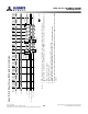

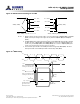
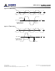

Table Of Contents
- DDR3L SDRAM
- Description
- State Diagram
- Functional Description
- Functional Block Diagrams
- Ball Assignments and Descriptions
- Package Dimensions
- Electrical Specifications
- Thermal Characteristics
- Electrical Specifications – I DD Specifications and Conditions
- Electrical Characteristics – 1.35V IDD Specifications
- Electrical Specifications – DC and AC
- ODT Characteristics
- Output Driver Impedance
- Output Characteristics and Operating Conditions
- Speed Bin Tables
- Electrical Characteristics and AC Operating Conditions
- Electrical Characteristics and AC Operating Conditions
- Command and Address Setup, Hold, and Derating
- Data Setup, Hold, and Derating
- Commands – Truth Tables
- Commands
- Input Clock Frequency Change
- Write Leveling
- Initialization
- Voltage Initialization / Change
- Mode Registers
- Mode Register 0 (MR0)
- Mode Register 1 (MR1)
- Mode Register 2 (MR2)
- Mode Register 3 (MR3)
- MODE REGISTER SET (MRS) Command
- ZQ CALIBRATION Operation
- ACTIVATE Operation
- READ Operation
- WRITE Operation
- PRECHARGE Operation
- SELF REFRESH Operation
- Extended Temperature Usage
- Power-Down Mode
- RESET Operation
- On-Die Termination (ODT)
- Dynamic ODT
- Synchronous ODT Mode
- Asynchronous ODT Mode
- Asynchronous to Synchronous ODT Mode Transition (Power-Down Exit)
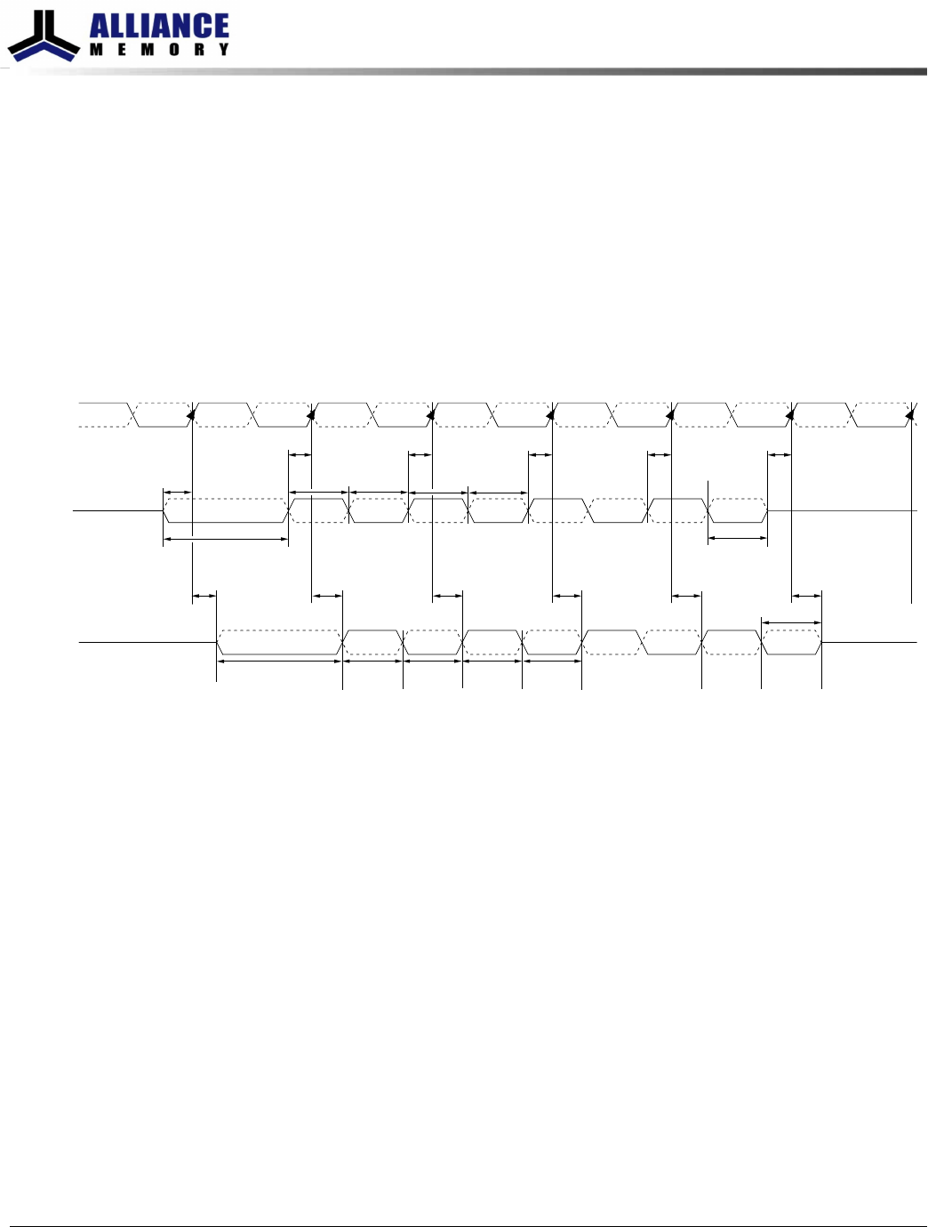
t
HZ and
t
LZ transitions occur in the same access time as valid data transitions. These
parameters are referenced to a specific voltage level that specifies when the device out-
put is no longer driving
t
HZDQS and
t
HZDQ, or begins driving
t
LZDQS,
t
LZDQ. Fig-
ure 77 (page 162) shows a method of calculating the point when the device is no longer
driving
t
HZDQS and
t
HZDQ, or begins driving
t
LZDQS,
t
LZDQ, by measuring the signal
at two different voltages. The actual voltage measurement points are not critical as long
as the calculation is consistent. The parameters
t
LZDQS,
t
LZDQ,
t
HZDQS, and
t
HZDQ
are defined as single-ended.
Figure 76: Data Strobe Timing – READs
RL measured
to this point
DQS, DQS#
early strobe
CK
t
LZDQS (MIN)
t
HZDQS (MIN)
DQS, DQS#
late strobe
t
LZDQS (MAX)
t
HZDQS (MAX)
t
DQSCK (MAX)
t
DQSCK (MAX)
t
DQSCK (MAX)
t
DQSCK (MAX)
t
DQSCK (MIN)
t
DQSCK (MIN)
t
DQSCK (MIN)
t
DQSCK (MIN)
CK#
t
RPRE
t
QSH
t
QSH
t
QSL
t
QSL
t
QSL
t
QSL
t
QSH
t
QSH
Bit 0 Bit 1 Bit 2 Bit 7
t
RPRE
Bit 0 Bit 1 Bit 2 Bit 7Bit 6Bit 3 Bit 4 Bit 5
Bit 6Bit 4Bit 3 Bit 5
t
RPST
t
RPST
T0 T1 T2 T3 T4 T5 T6
8Gb: x4, x8, x16 DDR3L SDRAM
READ Operation
161
Rev 2.0 June 2016
© 2015 Alliance Memory, Inc. All rights reserved.
Alliance Memory Inc. reserves the right to change products or specification without notice
Alliance Memory Inc. 511 Taylor Way, San Carlos, CA 94070
TEL: (650) 610-6800 FAX: (650) 620-9211