
Datasheet

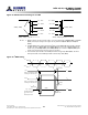
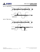

Table Of Contents
- DDR3L SDRAM
- Description
- State Diagram
- Functional Description
- Functional Block Diagrams
- Ball Assignments and Descriptions
- Package Dimensions
- Electrical Specifications
- Thermal Characteristics
- Electrical Specifications – I DD Specifications and Conditions
- Electrical Characteristics – 1.35V IDD Specifications
- Electrical Specifications – DC and AC
- ODT Characteristics
- Output Driver Impedance
- Output Characteristics and Operating Conditions
- Speed Bin Tables
- Electrical Characteristics and AC Operating Conditions
- Electrical Characteristics and AC Operating Conditions
- Command and Address Setup, Hold, and Derating
- Data Setup, Hold, and Derating
- Commands – Truth Tables
- Commands
- Input Clock Frequency Change
- Write Leveling
- Initialization
- Voltage Initialization / Change
- Mode Registers
- Mode Register 0 (MR0)
- Mode Register 1 (MR1)
- Mode Register 2 (MR2)
- Mode Register 3 (MR3)
- MODE REGISTER SET (MRS) Command
- ZQ CALIBRATION Operation
- ACTIVATE Operation
- READ Operation
- WRITE Operation
- PRECHARGE Operation
- SELF REFRESH Operation
- Extended Temperature Usage
- Power-Down Mode
- RESET Operation
- On-Die Termination (ODT)
- Dynamic ODT
- Synchronous ODT Mode
- Asynchronous ODT Mode
- Asynchronous to Synchronous ODT Mode Transition (Power-Down Exit)
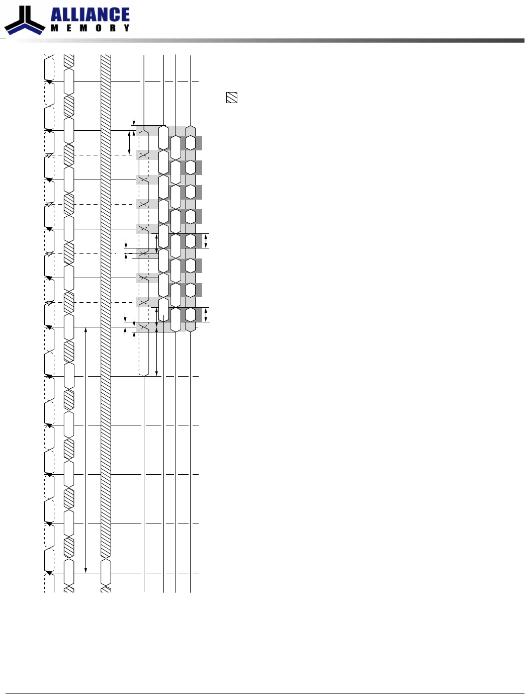
Figure 75: Data Output Timing –
t
DQSQ and Data Valid Window
T0 T1 T2 T3 T4 T5 T6 T7 T8 T9 T10
Bank,
Col n
t
RPST
NOPREAD NOPNOP NOP NOP NOP NOP NOP NOP NOP
CK
CK#
Command
1
Address
2
t
DQSQ (MAX)
DQS, DQS#
DQ
3
(last data valid)
DQ
3
(first data no longer valid)
All DQ collectively
DO
n
DO
n + 3
DO
n + 2
DO
n + 1
DO
n + 7
DO
n + 6
DO
n + 5
DO
n + 4
DO
n + 2
DO
n + 1
DO
n + 7
DO
n + 6
DO
n + 5
DO
n + 4
DO
n + 3
DO
n + 2
DO
n + 1
DO
n
DO
n + 7
DO
n + 6
DO
n + 5
DO
n
DO
n + 3
t
RPRE
Don’t Care
Data valid Data valid
t
QH
t
QH
t
HZ
DQ (MAX)
DO
n + 4
RL = AL + CL
t
DQSQ (MAX)
t
LZ
DQ (MIN)
Notes:
1. NOP commands are shown for ease of illustration; other commands may be valid at these times.
2. The BL8 setting is activated by either MR0[1, 0] = 0, 0 or MR0[0, 1] = 0, 1 and A12 = 1 during READ command at
T0.
3. DO n = data-out from column n.
4. BL8, RL = 5 (AL = 0, CL = 5).
5. Output timings are referenced to V
DDQ
/2 and DLL on and locked.
6.
t
DQSQ defines the skew between DQS, DQS# to data and does not define DQS, DQS# to CK.
7. Early data transitions may not always happen at the same DQ. Data transitions of a DQ can be early or late within
a burst.
8Gb: x4, x8, x16 DDR3L SDRAM
READ Operation
160
Rev 2.0 June 2016
© 2015 Alliance Memory, Inc. All rights reserved.
Alliance Memory Inc. reserves the right to change products or specification without notice
Alliance Memory Inc. 511 Taylor Way, San Carlos, CA 94070
TEL: (650) 610-6800 FAX: (650) 620-9211