
Datasheet
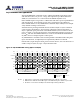
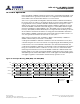
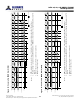
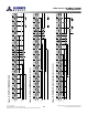

Table Of Contents
- DDR3L SDRAM
- Description
- State Diagram
- Functional Description
- Functional Block Diagrams
- Ball Assignments and Descriptions
- Package Dimensions
- Electrical Specifications
- Thermal Characteristics
- Electrical Specifications – I DD Specifications and Conditions
- Electrical Characteristics – 1.35V IDD Specifications
- Electrical Specifications – DC and AC
- ODT Characteristics
- Output Driver Impedance
- Output Characteristics and Operating Conditions
- Speed Bin Tables
- Electrical Characteristics and AC Operating Conditions
- Electrical Characteristics and AC Operating Conditions
- Command and Address Setup, Hold, and Derating
- Data Setup, Hold, and Derating
- Commands – Truth Tables
- Commands
- Input Clock Frequency Change
- Write Leveling
- Initialization
- Voltage Initialization / Change
- Mode Registers
- Mode Register 0 (MR0)
- Mode Register 1 (MR1)
- Mode Register 2 (MR2)
- Mode Register 3 (MR3)
- MODE REGISTER SET (MRS) Command
- ZQ CALIBRATION Operation
- ACTIVATE Operation
- READ Operation
- WRITE Operation
- PRECHARGE Operation
- SELF REFRESH Operation
- Extended Temperature Usage
- Power-Down Mode
- RESET Operation
- On-Die Termination (ODT)
- Dynamic ODT
- Synchronous ODT Mode
- Asynchronous ODT Mode
- Asynchronous to Synchronous ODT Mode Transition (Power-Down Exit)
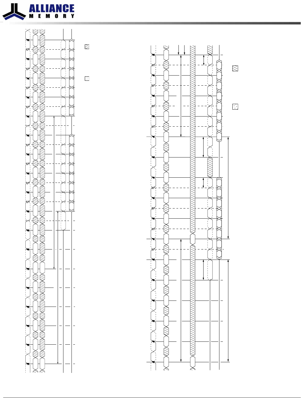
Figure 68: Nonconsecutive READ Bursts
Don’t CareTransitioning Data
T0 T1 T2 T3 T4 T5 T6 T7 T8 T9 T10 T11 T12 T13 T14 T15 T16 T17
DQS, DQS#
Command NOP NOP NOP NOP NOP NOP NOP NOP NOP NOP NOP NOP NOP NOPNOPREAD NOP READ
Address
Bank a,
Col n
Bank a,
Col b
CK
CK#
DQ
DO
n
DO
b
CL = 8
CL = 8
Notes:
1. AL = 0, RL = 8.
2. DO n (or b) = data-out from column n (or column b).
3. Seven subsequent elements of data-out appear in the programmed order following DO n.
4. Seven subsequent elements of data-out appear in the programmed order following DO b.
Figure 69: READ (BL8) to WRITE (BL8)
Don’t CareTransitioning Data
T0 T1 T2 T3 T4 T5 T6 T7 T8 T9 T10 T11 T12 T13 T14 T15
CK
CK#
Command
1
NOP NOP NOP NOP NOP WRITE NOP NOP NOP NOP NOP NOP NOP NOP NOP
t
WPST
t
RPRE
t
WPRE
t
RPST
DQS, DQS#
DQ
3
WL = 5
t
WR
t
WR
READ
DO
n
DO
n + 1
DO
n + 2
DO
n + 3
DO
n + 4
DO
n + 5
DO
n + 6
DO
n + 7
DI
n
DI
n + 1
DI
n + 2
DI
n + 3
DI
n + 4
DI
n + 5
DI
n + 6
DI
n + 7
READ-to-WRITE command delay = RL +
t
CCD + 2
t
CK - WL
t
BL = 4 clocks
Address
2
Bank,
Col b
Bank,
Col n
RL = 5
Notes:
1. NOP commands are shown for ease of illustration; other commands may be valid at these times.
2. The BL8 setting is activated by either MR0[1:0] = 00 or MR0[1:0] = 01 and A12 = 1 during the READ command at
T0, and the WRITE command at T6.
3. DO n = data-out from column, DI b = data-in for column b.
4. BL8, RL = 5 (AL = 0, CL = 5), WL = 5 (AL = 0, CWL = 5).
8Gb: x4, x8, x16 DDR3L SDRAM
READ Operation
156
Rev 2.0 June 2016
© 2015 Alliance Memory, Inc. All rights reserved.
Alliance Memory Inc. reserves the right to change products or specification without notice
Alliance Memory Inc. 511 Taylor Way, San Carlos, CA 94070
TEL: (650) 610-6800 FAX: (650) 620-9211