
Datasheet
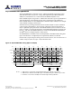
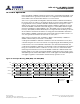
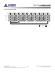
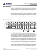
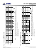
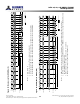
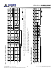

Table Of Contents
- DDR3L SDRAM
- Description
- State Diagram
- Functional Description
- Functional Block Diagrams
- Ball Assignments and Descriptions
- Package Dimensions
- Electrical Specifications
- Thermal Characteristics
- Electrical Specifications – I DD Specifications and Conditions
- Electrical Characteristics – 1.35V IDD Specifications
- Electrical Specifications – DC and AC
- ODT Characteristics
- Output Driver Impedance
- Output Characteristics and Operating Conditions
- Speed Bin Tables
- Electrical Characteristics and AC Operating Conditions
- Electrical Characteristics and AC Operating Conditions
- Command and Address Setup, Hold, and Derating
- Data Setup, Hold, and Derating
- Commands – Truth Tables
- Commands
- Input Clock Frequency Change
- Write Leveling
- Initialization
- Voltage Initialization / Change
- Mode Registers
- Mode Register 0 (MR0)
- Mode Register 1 (MR1)
- Mode Register 2 (MR2)
- Mode Register 3 (MR3)
- MODE REGISTER SET (MRS) Command
- ZQ CALIBRATION Operation
- ACTIVATE Operation
- READ Operation
- WRITE Operation
- PRECHARGE Operation
- SELF REFRESH Operation
- Extended Temperature Usage
- Power-Down Mode
- RESET Operation
- On-Die Termination (ODT)
- Dynamic ODT
- Synchronous ODT Mode
- Asynchronous ODT Mode
- Asynchronous to Synchronous ODT Mode Transition (Power-Down Exit)

Figure 68 (page 156). DDR3 SDRAM does not allow interrupting or truncating any
READ burst.
Data from any READ burst must be completed before a subsequent WRITE burst is al-
lowed. An example of a READ burst followed by a WRITE burst for BL8 is shown in Fig-
ure 69 (page 156) (BC4 is shown in Figure 70 (page 157)). To ensure the READ data is
completed before the WRITE data is on the bus, the minimum READ-to-WRITE timing
is RL +
t
CCD - WL + 2
t
CK.
A READ burst may be followed by a PRECHARGE command to the same bank, provided
auto precharge is not activated. The minimum READ-to-PRECHARGE command spac-
ing to the same bank is four clocks and must also satisfy a minimum analog time from
the READ command. This time is called
t
RTP (READ-to-PRECHARGE).
t
RTP starts AL
cycles later than the READ command. Examples for BL8 are shown in Figure 71
(page 157) and BC4 in Figure 72 (page 158). Following the PRECHARGE command, a
subsequent command to the same bank cannot be issued until
t
RP is met. The PRE-
CHARGE command followed by another PRECHARGE command to the same bank is al-
lowed. However, the precharge period will be determined by the last PRECHARGE com-
mand issued to the bank.
If A10 is HIGH when a READ command is issued, the READ with auto precharge func-
tion is engaged. The DRAM starts an auto precharge operation on the rising edge, which
is AL +
t
RTP cycles after the READ command. DRAM support a
t
RAS lockout feature (see
Figure 74 (page 158)). If
t
RAS (MIN) is not satisfied at the edge, the starting point of the
auto precharge operation will be delayed until
t
RAS (MIN) is satisfied. If
t
RTP (MIN) is
not satisfied at the edge, the starting point of the auto precharge operation is delayed
until
t
RTP (MIN) is satisfied. In case the internal precharge is pushed out by
t
RTP,
t
RP
starts at the point at which the internal precharge happens (not at the next rising clock
edge after this event). The time from READ with auto precharge to the next ACTIVATE
command to the same bank is AL + (
t
RTP +
t
RP)*, where * means rounded up to the next
integer. In any event, internal precharge does not start earlier than four clocks after the
last 8n-bit prefetch.
8Gb: x4, x8, x16 DDR3L SDRAM
READ Operation
154
Rev 2.0 June 2016
© 2015 Alliance Memory, Inc. All rights reserved.
Alliance Memory Inc. reserves the right to change products or specification without notice
Alliance Memory Inc. 511 Taylor Way, San Carlos, CA 94070
TEL: (650) 610-6800 FAX: (650) 620-9211