
Datasheet
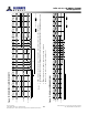

Table Of Contents
- DDR3L SDRAM
- Description
- State Diagram
- Functional Description
- Functional Block Diagrams
- Ball Assignments and Descriptions
- Package Dimensions
- Electrical Specifications
- Thermal Characteristics
- Electrical Specifications – I DD Specifications and Conditions
- Electrical Characteristics – 1.35V IDD Specifications
- Electrical Specifications – DC and AC
- ODT Characteristics
- Output Driver Impedance
- Output Characteristics and Operating Conditions
- Speed Bin Tables
- Electrical Characteristics and AC Operating Conditions
- Electrical Characteristics and AC Operating Conditions
- Command and Address Setup, Hold, and Derating
- Data Setup, Hold, and Derating
- Commands – Truth Tables
- Commands
- Input Clock Frequency Change
- Write Leveling
- Initialization
- Voltage Initialization / Change
- Mode Registers
- Mode Register 0 (MR0)
- Mode Register 1 (MR1)
- Mode Register 2 (MR2)
- Mode Register 3 (MR3)
- MODE REGISTER SET (MRS) Command
- ZQ CALIBRATION Operation
- ACTIVATE Operation
- READ Operation
- WRITE Operation
- PRECHARGE Operation
- SELF REFRESH Operation
- Extended Temperature Usage
- Power-Down Mode
- RESET Operation
- On-Die Termination (ODT)
- Dynamic ODT
- Synchronous ODT Mode
- Asynchronous ODT Mode
- Asynchronous to Synchronous ODT Mode Transition (Power-Down Exit)
ACTIVATE Operation
Before any READ or WRITE commands can be issued to a bank within the DRAM, a row
in that bank must be opened (activated). This is accomplished via the ACTIVATE com-
mand, which selects both the bank and the row to be activated.
After a row is opened with an ACTIVATE command, a READ or WRITE command may
be issued to that row, subject to the
t
RCD specification. However, if the additive latency
is programmed correctly, a READ or WRITE command may be issued prior to
t
RCD
(MIN). In this operation, the DRAM enables a READ or WRITE command to be issued
after the ACTIVATE command for that bank, but prior to
t
RCD (MIN) with the require-
ment that (ACTIVATE-to-READ/WRITE) + AL ≥
t
RCD (MIN) (see Posted CAS Additive
Latency).
t
RCD (MIN) should be divided by the clock period and rounded up to the next
whole number to determine the earliest clock edge after the ACTIVATE command on
which a READ or WRITE command can be entered. The same procedure is used to con-
vert other specification limits from time units to clock cycles.
When at least one bank is open, any READ-to-READ command delay or WRITE-to-
WRITE command delay is restricted to
t
CCD (MIN).
A subsequent ACTIVATE command to a different row in the same bank can only be is-
sued after the previous active row has been closed (precharged). The minimum time in-
terval between successive ACTIVATE commands to the same bank is defined by
t
RC.
A subsequent ACTIVATE command to another bank can be issued while the first bank is
being accessed, which results in a reduction of total row-access overhead. The mini-
mum time interval between successive ACTIVATE commands to different banks is de-
fined by
t
RRD. No more than four bank ACTIVATE commands may be issued in a given
t
FAW (MIN) period, and the
t
RRD (MIN) restriction still applies. The
t
FAW (MIN) param-
eter applies, regardless of the number of banks already opened or closed.
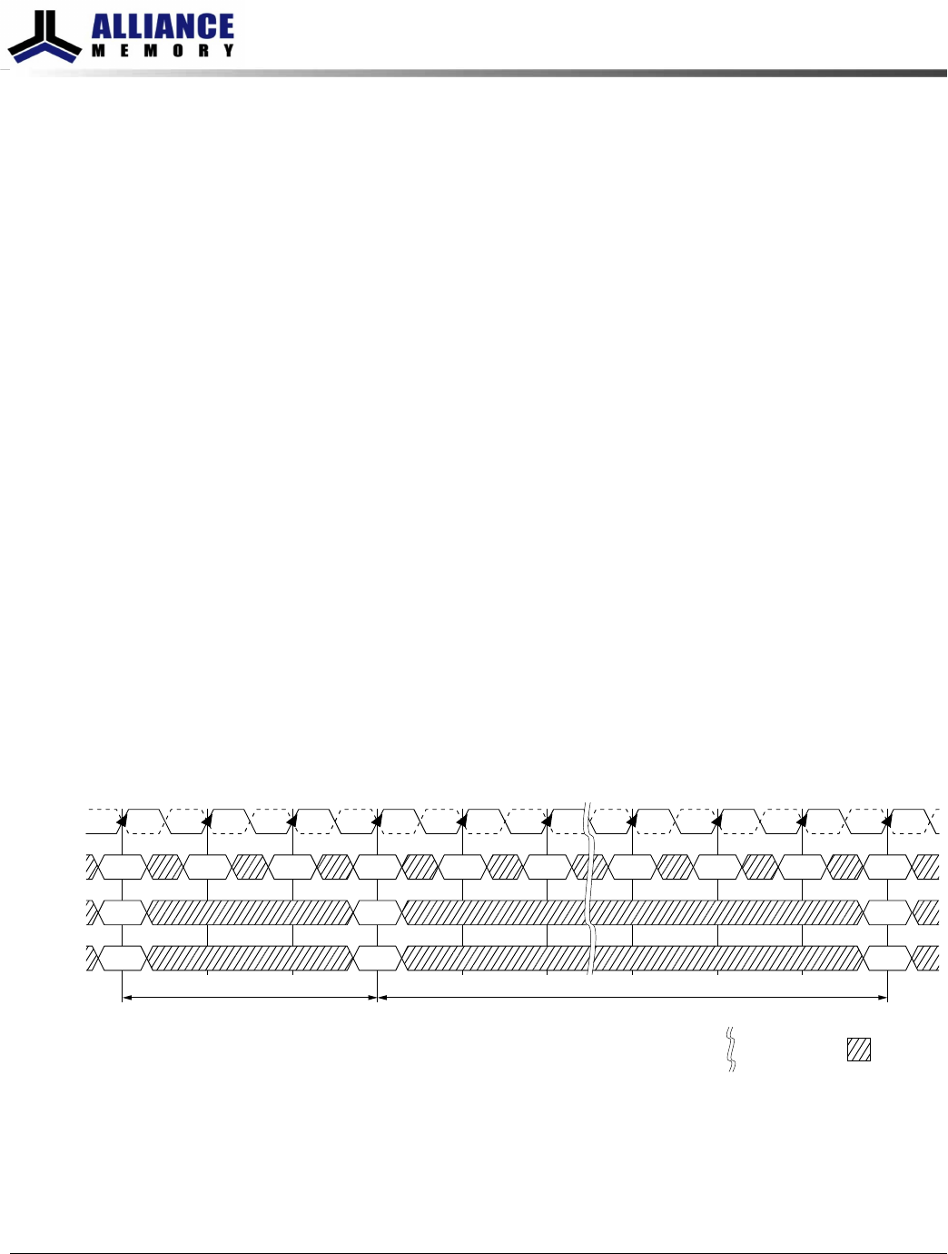
Figure 63: Example: Meeting
t
RRD (MIN) and
t
RCD (MIN)
Command
Don’t Care
T1T0 T2 T3 T4 T5 T8 T9
t
RRD
Row Row
Col
Bank x Bank y
Bank y
NOPACT NOP NOPACT NOP NOP RD/WR
t
RCD
BA[2:0]
CK#
Address
CK
T10
T11
NOP
NOP
Indicates break
in time scale
8Gb: x4, x8, x16 DDR3L SDRAM
ACTIVATE Operation
151
Rev 2.0 June 2016
© 2015 Alliance Memory, Inc. All rights reserved.
Alliance Memory Inc. reserves the right to change products or specification without notice
Alliance Memory Inc. 511 Taylor Way, San Carlos, CA 94070
TEL: (650) 610-6800 FAX: (650) 620-9211