
Datasheet
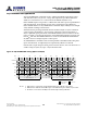
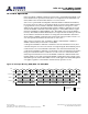
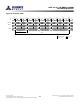
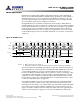
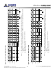
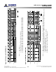
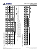

Table Of Contents
- DDR3L SDRAM
- Description
- State Diagram
- Functional Description
- Functional Block Diagrams
- Ball Assignments and Descriptions
- Package Dimensions
- Electrical Specifications
- Thermal Characteristics
- Electrical Specifications – I DD Specifications and Conditions
- Electrical Characteristics – 1.35V IDD Specifications
- Electrical Specifications – DC and AC
- ODT Characteristics
- Output Driver Impedance
- Output Characteristics and Operating Conditions
- Speed Bin Tables
- Electrical Characteristics and AC Operating Conditions
- Electrical Characteristics and AC Operating Conditions
- Command and Address Setup, Hold, and Derating
- Data Setup, Hold, and Derating
- Commands – Truth Tables
- Commands
- Input Clock Frequency Change
- Write Leveling
- Initialization
- Voltage Initialization / Change
- Mode Registers
- Mode Register 0 (MR0)
- Mode Register 1 (MR1)
- Mode Register 2 (MR2)
- Mode Register 3 (MR3)
- MODE REGISTER SET (MRS) Command
- ZQ CALIBRATION Operation
- ACTIVATE Operation
- READ Operation
- WRITE Operation
- PRECHARGE Operation
- SELF REFRESH Operation
- Extended Temperature Usage
- Power-Down Mode
- RESET Operation
- On-Die Termination (ODT)
- Dynamic ODT
- Synchronous ODT Mode
- Asynchronous ODT Mode
- Asynchronous to Synchronous ODT Mode Transition (Power-Down Exit)
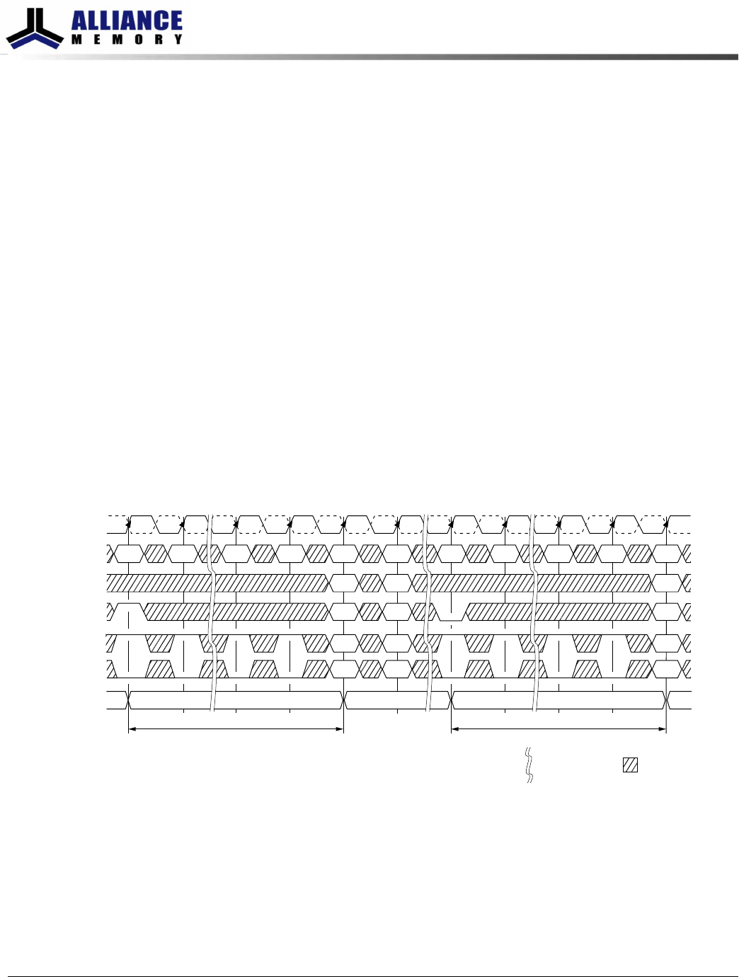
ZQ CALIBRATION Operation
The ZQ CALIBRATION command is used to calibrate the DRAM output drivers (R
ON
)
and ODT values (R
TT
) over process, voltage, and temperature, provided a dedicated
240Ω (±1%) external resistor is connected from the DRAM’s ZQ ball to V
SSQ
.
DDR3 SDRAM require a longer time to calibrate R
ON
and ODT at power-up initialization
and self refresh exit, and a relatively shorter time to perform periodic calibrations.
DDR3 SDRAM defines two ZQ CALIBRATION commands: ZQCL and ZQCS. An example
of ZQ calibration timing is shown below.
All banks must be precharged and
t
RP must be met before ZQCL or ZQCS commands
can be issued to the DRAM. No other activities (other than issuing another ZQCL or
ZQCS command) can be performed on the DRAM channel by the controller for the du-
ration of
t
ZQinit or
t
ZQoper. The quiet time on the DRAM channel helps accurately cali-
brate R
ON
and ODT. After DRAM calibration is achieved, the DRAM should disable the
ZQ ball’s current consumption path to reduce power.
ZQ CALIBRATION commands can be issued in parallel to DLL RESET and locking time.
Upon self refresh exit, an explicit ZQCL is required if ZQ calibration is desired.
In dual-rank systems that share the ZQ resistor between devices, the controller must not
enable overlap of
t
ZQinit,
t
ZQoper, or
t
ZQCS between ranks.
Figure 62: ZQ CALIBRATION Timing (ZQCL and ZQCS)
NOPZQCL NOP NOP Valid Valid ZQCS NOP NOP NOP ValidCommand
Indicates break
in time scale
T0 T1 Ta0 Ta1 Ta2 Ta3 Tb0 Tb1 Tc0 Tc1 Tc2
Address Valid ValidValid
A10
Valid ValidValid
CK
CK#
Don’t Care
DQ High-Z High-Z33 Activities
Activ-
ities
Valid ValidODT 2 2 Valid
1
CKE
1 Valid Valid Valid
t
ZQCS
t
ZQinit or
t
ZQoper
Notes:
1. CKE must be continuously registered HIGH during the calibration procedure.
2. ODT must be disabled via the ODT signal or the MRS during the calibration procedure.
3. All devices connected to the DQ bus should be High-Z during calibration.
8Gb: x4, x8, x16 DDR3L SDRAM
ZQ CALIBRATION Operation
150
Rev 2.0 June 2016
© 2015 Alliance Memory, Inc. All rights reserved.
Alliance Memory Inc. reserves the right to change products or specification without notice
Alliance Memory Inc. 511 Taylor Way, San Carlos, CA 94070
TEL: (650) 610-6800 FAX: (650) 620-9211