
Datasheet
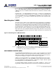
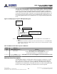
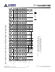
Table Of Contents
- DDR3L SDRAM
- Description
- State Diagram
- Functional Description
- Functional Block Diagrams
- Ball Assignments and Descriptions
- Package Dimensions
- Electrical Specifications
- Thermal Characteristics
- Electrical Specifications – I DD Specifications and Conditions
- Electrical Characteristics – 1.35V IDD Specifications
- Electrical Specifications – DC and AC
- ODT Characteristics
- Output Driver Impedance
- Output Characteristics and Operating Conditions
- Speed Bin Tables
- Electrical Characteristics and AC Operating Conditions
- Electrical Characteristics and AC Operating Conditions
- Command and Address Setup, Hold, and Derating
- Data Setup, Hold, and Derating
- Commands – Truth Tables
- Commands
- Input Clock Frequency Change
- Write Leveling
- Initialization
- Voltage Initialization / Change
- Mode Registers
- Mode Register 0 (MR0)
- Mode Register 1 (MR1)
- Mode Register 2 (MR2)
- Mode Register 3 (MR3)
- MODE REGISTER SET (MRS) Command
- ZQ CALIBRATION Operation
- ACTIVATE Operation
- READ Operation
- WRITE Operation
- PRECHARGE Operation
- SELF REFRESH Operation
- Extended Temperature Usage
- Power-Down Mode
- RESET Operation
- On-Die Termination (ODT)
- Dynamic ODT
- Synchronous ODT Mode
- Asynchronous ODT Mode
- Asynchronous to Synchronous ODT Mode Transition (Power-Down Exit)

MPR Read Predefined Pattern
The predetermined read calibration pattern is a fixed pattern of 0, 1, 0, 1, 0, 1, 0, 1. The
following is an example of using the read out predetermined read calibration pattern.
The example is to perform multiple reads from the multipurpose register to do system
level read timing calibration based on the predetermined and standardized pattern.
The following protocol outlines the steps used to perform the read calibration:
1. Precharge all banks
2. After
t
RP is satisfied, set MRS, MR3[2] = 1 and MR3[1:0] = 00. This redirects all sub-
sequent reads and loads the predefined pattern into the MPR. As soon as
t
MRD
and
t
MOD are satisfied, the MPR is available
3. Data WRITE operations are not allowed until the MPR returns to the normal
DRAM state
4. Issue a read with burst order information (all other address pins are “Don’t Care”):
• A[1:0] = 00 (data burst order is fixed starting at nibble)
• A2 = 0 (for BL8, burst order is fixed as 0, 1, 2, 3, 4, 5, 6, 7)
• A12 = 1 (use BL8)
5. After RL = AL + CL, the DRAM bursts out the predefined read calibration pattern
(0, 1, 0, 1, 0, 1, 0, 1)
6. The memory controller repeats the calibration reads until read data capture at
memory controller is optimized
7. After the last MPR READ burst and after
t
MPRR has been satisfied, issue MRS,
MR3[2] = 0, and MR3[1:0] = “Don’t Care” to the normal DRAM state. All subse-
quent read and write accesses will be regular reads and writes from/to the DRAM
array
8. When
t
MRD and
t
MOD are satisfied from the last MRS, the regular DRAM com-
mands (such as activate a memory bank for regular read or write access) are per-
mitted
MODE REGISTER SET (MRS) Command
The mode registers are loaded via inputs BA[2:0], A[13:0]. BA[2:0] determine which
mode register is programmed:
• BA2 = 0, BA1 = 0, BA0 = 0 for MR0
• BA2 = 0, BA1 = 0, BA0 = 1 for MR1
• BA2 = 0, BA1 = 1, BA0 = 0 for MR2
• BA2 = 0, BA1 = 1, BA0 = 1 for MR3
The MRS command can only be issued (or re-issued) when all banks are idle and in the
precharged state (
t
RP is satisfied and no data bursts are in progress). The controller
must wait the specified time
t
MRD before initiating a subsequent operation such as an
ACTIVATE command (see Figure 48 (page 130)). There is also a restriction after issuing
an MRS command with regard to when the updated functions become available. This
parameter is specified by
t
MOD. Both
t
MRD and
t
MOD parameters are shown in Fig-
ure 48 (page 130) and Figure 49 (page 131). Violating either of these requirements will
result in unspecified operation.
8Gb: x4, x8, x16 DDR3L SDRAM
MODE REGISTER SET (MRS) Command
149
Rev 2.0 June 2016
© 2015 Alliance Memory, Inc. All rights reserved.
Alliance Memory Inc. reserves the right to change products or specification without notice
Alliance Memory Inc. 511 Taylor Way, San Carlos, CA 94070
TEL: (650) 610-6800 FAX: (650) 620-9211