
Datasheet
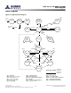
Table Of Contents
- DDR3L SDRAM
- Description
- State Diagram
- Functional Description
- Functional Block Diagrams
- Ball Assignments and Descriptions
- Package Dimensions
- Electrical Specifications
- Thermal Characteristics
- Electrical Specifications – I DD Specifications and Conditions
- Electrical Characteristics – 1.35V IDD Specifications
- Electrical Specifications – DC and AC
- ODT Characteristics
- Output Driver Impedance
- Output Characteristics and Operating Conditions
- Speed Bin Tables
- Electrical Characteristics and AC Operating Conditions
- Electrical Characteristics and AC Operating Conditions
- Command and Address Setup, Hold, and Derating
- Data Setup, Hold, and Derating
- Commands – Truth Tables
- Commands
- Input Clock Frequency Change
- Write Leveling
- Initialization
- Voltage Initialization / Change
- Mode Registers
- Mode Register 0 (MR0)
- Mode Register 1 (MR1)
- Mode Register 2 (MR2)
- Mode Register 3 (MR3)
- MODE REGISTER SET (MRS) Command
- ZQ CALIBRATION Operation
- ACTIVATE Operation
- READ Operation
- WRITE Operation
- PRECHARGE Operation
- SELF REFRESH Operation
- Extended Temperature Usage
- Power-Down Mode
- RESET Operation
- On-Die Termination (ODT)
- Dynamic ODT
- Synchronous ODT Mode
- Asynchronous ODT Mode
- Asynchronous to Synchronous ODT Mode Transition (Power-Down Exit)
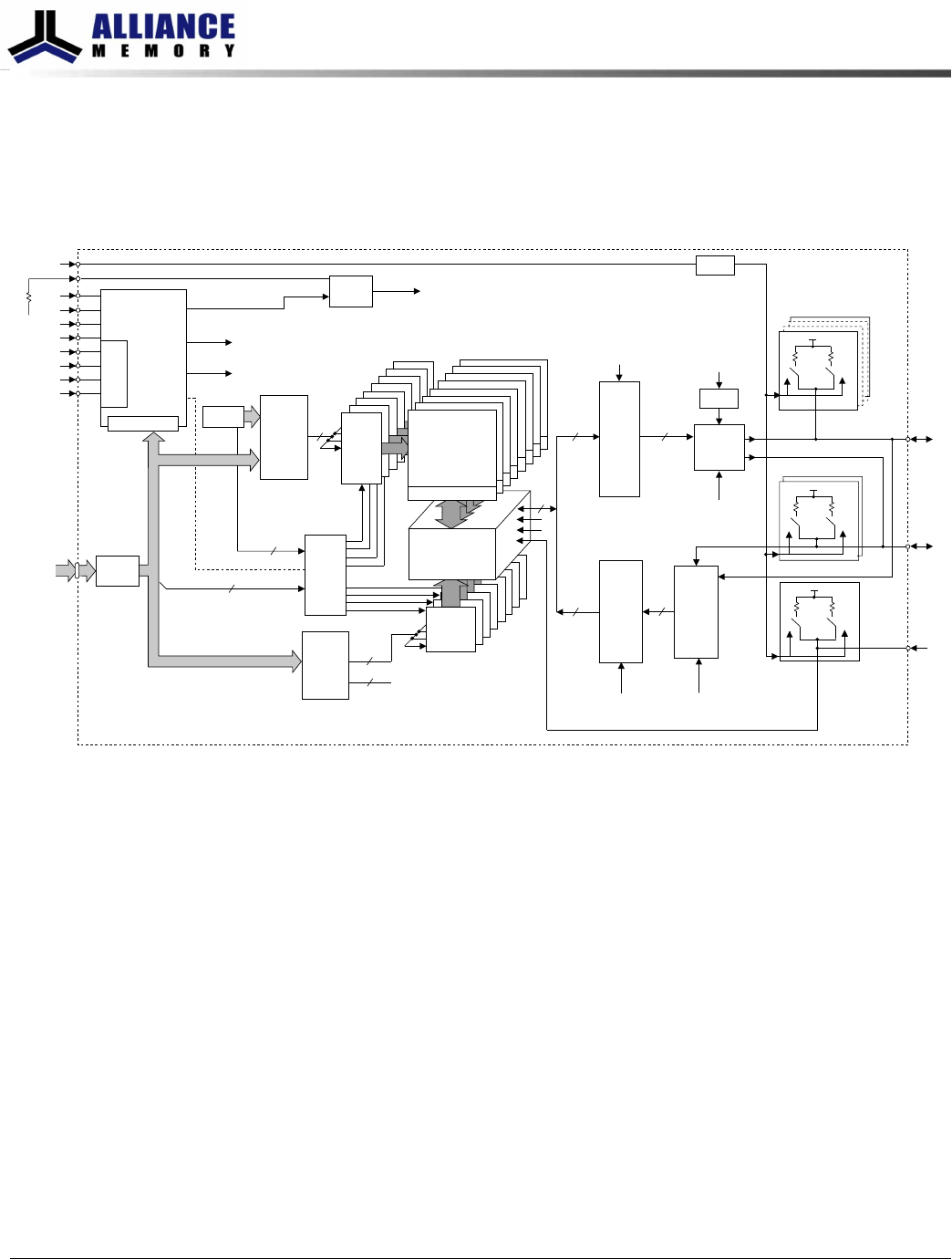
Functional Block Diagrams
DDR3 SDRAM is a high-speed, CMOS dynamic random access memory. It is internally
configured as an 8-bank DRAM.
Figure 3: 2 Gig x 4 Functional Block Diagram
Bank 5
Bank 6
Bank 7
Bank 4
Bank 7
Bank 4
Bank 5
Bank 6
16
Row-
address
MUX
Control
logic
Column-
address
counter/
latch
Mode registers
12
Command
decode
A[15:0]
BA[2:0]
16
Address
register
19
512
(x32)
16,384
I/O gating
DM mask logic
Column
decoder
Bank 0
memory
array
(65,536 x 512 x 32)
Bank 0
row-
address
latch
and
decoder
65,536
Sense amplifiers
Bank
control
logic
19
Bank 1
Bank 2
Bank 3
16
9
3
3
Refresh
counter
4
32
32
32
DQS, DQS#
Columns 0, 1, and 2
Columns 0, 1, and 2
ZQCL, ZQCS
To pull-up/pull-down
networks
READ
drivers
DQ[3:0]
READ
FIFO
and
data
MUX
Data
4
3
Bank 1
Bank 2
Bank 3
DM
DM
CK, CK#
DQS, DQS#
ZQ CAL
CS#
ZQ
RZQ
CK, CK#
RAS#
WE#
CAS#
ODT
CKE
RESET#
CK, CK#
DLL
DQ[3:0]
(1 . . . 4)
(1, 2)
sw1
sw2
V
DDQ
/2
R
TT,nom
R
TT(WR)
sw1 sw2
V
DDQ
/2
R
TT,nom
R
TT(WR)
sw1
sw2
V
DDQ
/2
R
TT,nom
R
TT(WR)
OTF
BC4 (burst chop)
BC4
Column 2
(select upper or
lower nibble for BC4)
Data
interface
WRITE
drivers
and
input
logic
ODT
control
V
SSQ
A12
OTF
BC4
8Gb: x4, x8, x16 DDR3L SDRAM
Functional Block Diagrams
14
Rev 2.0 June 2016
© 2015 Alliance Memory, Inc. All rights reserved.
Alliance Memory Inc. reserves the right to change products or specification without notice
Alliance Memory Inc. 511 Taylor Way, San Carlos, CA 94070
TEL: (650) 610-6800 FAX: (650) 620-9211