
Datasheet
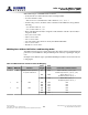
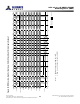
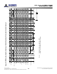
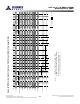
Table Of Contents
- DDR3L SDRAM
- Description
- State Diagram
- Functional Description
- Functional Block Diagrams
- Ball Assignments and Descriptions
- Package Dimensions
- Electrical Specifications
- Thermal Characteristics
- Electrical Specifications – I DD Specifications and Conditions
- Electrical Characteristics – 1.35V IDD Specifications
- Electrical Specifications – DC and AC
- ODT Characteristics
- Output Driver Impedance
- Output Characteristics and Operating Conditions
- Speed Bin Tables
- Electrical Characteristics and AC Operating Conditions
- Electrical Characteristics and AC Operating Conditions
- Command and Address Setup, Hold, and Derating
- Data Setup, Hold, and Derating
- Commands – Truth Tables
- Commands
- Input Clock Frequency Change
- Write Leveling
- Initialization
- Voltage Initialization / Change
- Mode Registers
- Mode Register 0 (MR0)
- Mode Register 1 (MR1)
- Mode Register 2 (MR2)
- Mode Register 3 (MR3)
- MODE REGISTER SET (MRS) Command
- ZQ CALIBRATION Operation
- ACTIVATE Operation
- READ Operation
- WRITE Operation
- PRECHARGE Operation
- SELF REFRESH Operation
- Extended Temperature Usage
- Power-Down Mode
- RESET Operation
- On-Die Termination (ODT)
- Dynamic ODT
- Synchronous ODT Mode
- Asynchronous ODT Mode
- Asynchronous to Synchronous ODT Mode Transition (Power-Down Exit)
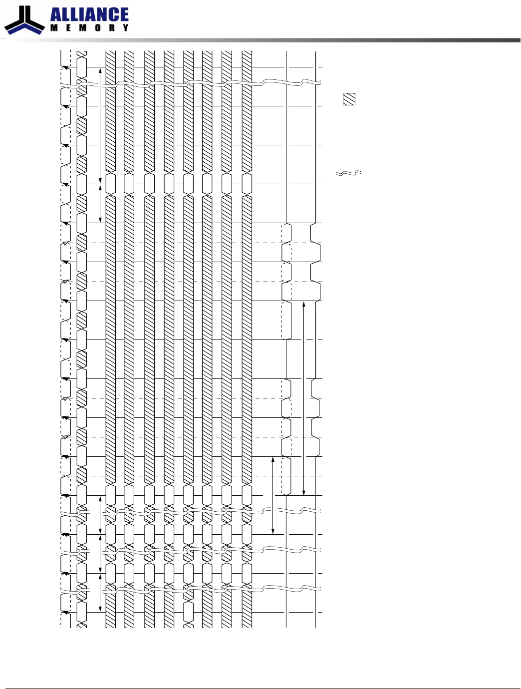
Figure 61: MPR System Read Calibration with BC4: Upper Nibble, Then Lower Nibble
T0 Ta Tb
01A10/AP Valid Valid 0
CK
CK#
MRSPREA
READ
1
READ
1
NOP NOP NOP NOP NOP NOP NOP MRS NOP NOP ValidCommand
0
0
4
1
3
1A2
t
MOD
t
MPRR
3 Valid 3Bank address Valid
0
2
0
2
0A[1:0] Valid
00A[15:13] Valid Valid
00A11 Valid Valid
0000A[9:3] Valid Valid
Don’t Care
Tc0 Tc1 Tc2 Tc3 Tc4 Tc5 Tc6 Tc7 Tc8 Tc9 Tc10 Td
Indicates break
in time scale
RL
DQ
DQS, DQS#
0A12/BC#
Valid
1
Valid
1
0
RL
t
RF
t
MOD
t
CCD
Notes:
1. READ with BC4 either by MRS or OTF.
2. Memory controller must drive 0 on A[1:0].
3. A2 = 1 selects upper 4 nibble bits 4 . . . 7.
4. A2 = 0 selects lower 4 nibble bits 0 . . . 3.
8Gb: x4, x8, x16 DDR3L SDRAM
Mode Register 3 (MR3)
148
Rev 2.0 June 2016
© 2015 Alliance Memory, Inc. All rights reserved.
Alliance Memory Inc. reserves the right to change products or specification without notice
Alliance Memory Inc. 511 Taylor Way, San Carlos, CA 94070
TEL: (650) 610-6800 FAX: (650) 620-9211