
Datasheet
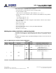
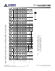
Table Of Contents
- DDR3L SDRAM
- Description
- State Diagram
- Functional Description
- Functional Block Diagrams
- Ball Assignments and Descriptions
- Package Dimensions
- Electrical Specifications
- Thermal Characteristics
- Electrical Specifications – I DD Specifications and Conditions
- Electrical Characteristics – 1.35V IDD Specifications
- Electrical Specifications – DC and AC
- ODT Characteristics
- Output Driver Impedance
- Output Characteristics and Operating Conditions
- Speed Bin Tables
- Electrical Characteristics and AC Operating Conditions
- Electrical Characteristics and AC Operating Conditions
- Command and Address Setup, Hold, and Derating
- Data Setup, Hold, and Derating
- Commands – Truth Tables
- Commands
- Input Clock Frequency Change
- Write Leveling
- Initialization
- Voltage Initialization / Change
- Mode Registers
- Mode Register 0 (MR0)
- Mode Register 1 (MR1)
- Mode Register 2 (MR2)
- Mode Register 3 (MR3)
- MODE REGISTER SET (MRS) Command
- ZQ CALIBRATION Operation
- ACTIVATE Operation
- READ Operation
- WRITE Operation
- PRECHARGE Operation
- SELF REFRESH Operation
- Extended Temperature Usage
- Power-Down Mode
- RESET Operation
- On-Die Termination (ODT)
- Dynamic ODT
- Synchronous ODT Mode
- Asynchronous ODT Mode
- Asynchronous to Synchronous ODT Mode Transition (Power-Down Exit)
MPR addressing for a valid MPR read is as follows:
• A[1:0] must be set to 00 as the burst order is fixed per nibble
• A2 selects the burst order:
– BL8, A2 is set to 0, and the burst order is fixed to 0, 1, 2, 3, 4, 5, 6, 7
• For burst chop 4 cases, the burst order is switched on the nibble base along with the
following:
– A2 = 0; burst order = 0, 1, 2, 3
– A2 = 1; burst order = 4, 5, 6, 7
• Burst order bit 0 (the first bit) is assigned to LSB, and burst order bit 7 (the last bit) is
assigned to MSB
• A[9:3] are a “Don’t Care”
• A10 is a “Don’t Care”
• A11 is a “Don’t Care”
• A12: Selects burst chop mode on-the-fly, if enabled within MR0
• A13 is a “Don’t Care”
• BA[2:0] are a “Don’t Care”
MPR Register Address Definitions and Bursting Order
The MPR currently supports a single data format. This data format is a predefined read
pattern for system calibration. The predefined pattern is always a repeating 0–1 bit pat-
tern.
Examples of the different types of predefined READ pattern bursts are shown in the fol-
lowing figures.
Table 75: MPR Readouts and Burst Order Bit Mapping
MR3[2] MR3[1:0] Function
Burst
Length
Read
A[2:0]
Burst Order and Data Pattern
1 00 READ predefined pattern
for system calibration
BL8 000 Burst order: 0, 1, 2, 3, 4, 5, 6, 7
Predefined pattern: 0, 1, 0, 1, 0, 1, 0, 1
BC4 000 Burst order: 0, 1, 2, 3
Predefined pattern: 0, 1, 0, 1
BC4 100 Burst order: 4, 5, 6, 7
Predefined pattern: 0, 1, 0, 1
1 01 RFU N/A N/A N/A
N/A N/A N/A
N/A N/A N/A
1 10 RFU N/A N/A N/A
N/A N/A N/A
N/A N/A N/A
8Gb: x4, x8, x16 DDR3L SDRAM
Mode Register 3 (MR3)
143
Rev 2.0 June 2016
© 2015 Alliance Memory, Inc. All rights reserved.
Alliance Memory Inc. reserves the right to change products or specification without notice
Alliance Memory Inc. 511 Taylor Way, San Carlos, CA 94070
TEL: (650) 610-6800 FAX: (650) 620-9211