
Datasheet
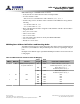
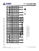
Table Of Contents
- DDR3L SDRAM
- Description
- State Diagram
- Functional Description
- Functional Block Diagrams
- Ball Assignments and Descriptions
- Package Dimensions
- Electrical Specifications
- Thermal Characteristics
- Electrical Specifications – I DD Specifications and Conditions
- Electrical Characteristics – 1.35V IDD Specifications
- Electrical Specifications – DC and AC
- ODT Characteristics
- Output Driver Impedance
- Output Characteristics and Operating Conditions
- Speed Bin Tables
- Electrical Characteristics and AC Operating Conditions
- Electrical Characteristics and AC Operating Conditions
- Command and Address Setup, Hold, and Derating
- Data Setup, Hold, and Derating
- Commands – Truth Tables
- Commands
- Input Clock Frequency Change
- Write Leveling
- Initialization
- Voltage Initialization / Change
- Mode Registers
- Mode Register 0 (MR0)
- Mode Register 1 (MR1)
- Mode Register 2 (MR2)
- Mode Register 3 (MR3)
- MODE REGISTER SET (MRS) Command
- ZQ CALIBRATION Operation
- ACTIVATE Operation
- READ Operation
- WRITE Operation
- PRECHARGE Operation
- SELF REFRESH Operation
- Extended Temperature Usage
- Power-Down Mode
- RESET Operation
- On-Die Termination (ODT)
- Dynamic ODT
- Synchronous ODT Mode
- Asynchronous ODT Mode
- Asynchronous to Synchronous ODT Mode Transition (Power-Down Exit)
back to ODT (R
TT,nom
) at the completion of the WRITE burst. If R
TT,nom
is disabled, the
R
TT,nom
value will be High-Z. Special timing parameters must be adhered to when dy-
namic ODT (R
TT(WR)
) is enabled: ODTLcnw, ODTLcnw4, ODTLcnw8, ODTH4, ODTH8,
and
t
ADC.
Dynamic ODT is only applicable during WRITE cycles. If ODT (R
TT,nom
) is disabled, dy-
namic ODT (R
TT(WR)
) is still permitted. R
TT,nom
and R
TT(WR)
can be used independent of
one other. Dynamic ODT is not available during write leveling mode, regardless of the
state of ODT (R
TT,nom
). For details on dynamic ODT operation, refer to Dynamic ODT
(page 189).
Mode Register 3 (MR3)
The mode register 3 (MR3) controls additional functions and features not available in
the other mode registers. Currently defined is the MULTIPURPOSE REGISTER (MPR).
This function is controlled via the bits shown in Figure 56 (page 141). The MR3 is pro-
grammed via the LOAD MODE command and retains the stored information until it is
programmed again or until the device loses power. Reprogramming the MR3 register
will not alter the contents of the memory array, provided it is performed correctly. The
MR3 register must be loaded when all banks are idle and no data bursts are in progress,
and the controller must wait the specified time
t
MRD and
t
MOD before initiating a sub-
sequent operation.
Figure 56: Mode Register 3 (MR3) Definition
A9 A7 A6 A5 A4 A3A8 A2 A1 A0
Mode register 3 (MR3)
Address bus
9765438210
A10A12 A11BA0BA1
101112131415
A13A14A15
0
1
0
1
0
1
0
1
0
1
0
1
0
1
0
1
0
1
MPR
11
BA2
161718
0
1
0
1
0
1
0
1
0
1
M2
0
1
MPR Enable
Normal DRAM operations
2
Dataflow from MPR
MPR_RF
M16
0
1
0
1
M17
0
0
1
1
Mode Register
Mode register set (MR0)
Mode register set 1 (MR1)
Mode register set 2 (MR2)
Mode register set 3 (MR3)
MPR READ Function
Predefined pattern
3
Reserved
Reserved
Reserved
M0
0
1
0
1
M1
0
0
1
1
Notes:
1. MR3[18 and 15:3] are reserved for future use and must all be programmed to 0.
2. When MPR control is set for normal DRAM operation, MR3[1, 0] will be ignored.
3. Intended to be used for READ synchronization.
MULTIPURPOSE REGISTER (MPR)
The MULTIPURPOSE REGISTER function is used to output a predefined system timing
calibration bit sequence. Bit 2 is the master bit that enables or disables access to the
MPR register, and bits 1 and 0 determine which mode the MPR is placed in. The basic
concept of the multipurpose register is shown in Figure 57 (page 142).
If MR3[2] is a 0, then the MPR access is disabled, and the DRAM operates in normal
mode. However, if MR3[2] is a 1, then the DRAM no longer outputs normal read data
but outputs MPR data as defined by MR3[0, 1]. If MR3[0, 1] is equal to 00, then a prede-
fined read pattern for system calibration is selected.
To enable the MPR, the MRS command is issued to MR3, and MR3[2] = 1. Prior to issu-
ing the MRS command, all banks must be in the idle state (all banks are precharged,
8Gb: x4, x8, x16 DDR3L SDRAM
Mode Register 3 (MR3)
141
Rev 2.0 June 2016
© 2015 Alliance Memory, Inc. All rights reserved.
Alliance Memory Inc. reserves the right to change products or specification without notice
Alliance Memory Inc. 511 Taylor Way, San Carlos, CA 94070
TEL: (650) 610-6800 FAX: (650) 620-9211