
Datasheet
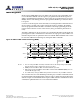
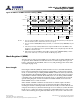

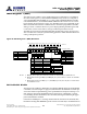
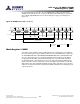
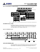
Table Of Contents
- DDR3L SDRAM
- Description
- State Diagram
- Functional Description
- Functional Block Diagrams
- Ball Assignments and Descriptions
- Package Dimensions
- Electrical Specifications
- Thermal Characteristics
- Electrical Specifications – I DD Specifications and Conditions
- Electrical Characteristics – 1.35V IDD Specifications
- Electrical Specifications – DC and AC
- ODT Characteristics
- Output Driver Impedance
- Output Characteristics and Operating Conditions
- Speed Bin Tables
- Electrical Characteristics and AC Operating Conditions
- Electrical Characteristics and AC Operating Conditions
- Command and Address Setup, Hold, and Derating
- Data Setup, Hold, and Derating
- Commands – Truth Tables
- Commands
- Input Clock Frequency Change
- Write Leveling
- Initialization
- Voltage Initialization / Change
- Mode Registers
- Mode Register 0 (MR0)
- Mode Register 1 (MR1)
- Mode Register 2 (MR2)
- Mode Register 3 (MR3)
- MODE REGISTER SET (MRS) Command
- ZQ CALIBRATION Operation
- ACTIVATE Operation
- READ Operation
- WRITE Operation
- PRECHARGE Operation
- SELF REFRESH Operation
- Extended Temperature Usage
- Power-Down Mode
- RESET Operation
- On-Die Termination (ODT)
- Dynamic ODT
- Synchronous ODT Mode
- Asynchronous ODT Mode
- Asynchronous to Synchronous ODT Mode Transition (Power-Down Exit)
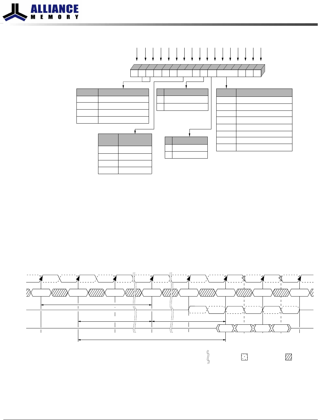
Figure 54: Mode Register 2 (MR2) Definition
M14
0
1
0
1
M15
0
0
1
1
Mode Register
Mode register set 0 (MR0)
Mode register set 1 (MR1)
Mode register set 2 (MR2)
Mode register set 3 (MR3)
A9 A7 A6 A5 A4 A3A8 A2 A1 A0
Mode register 2 (MR2)
Address bus
9765438210
A10A12 A11BA0BA1
101112131415
1
CWL
0
1
0
BA2
ASR
16
0
1
A13
0
1
0
1
0
1
0
1
0
1
0
1
SRT
R
TT(WR)
M6
0
1
Auto Self Refresh
Disabled: Manual
Enabled: Automatic
M7
0
1
Self Refresh Temperature
Normal (0°C to 85°C)
Extended (0°C to 95°C)
CAS Write Latency (CWL)
5 CK (
t
CK ≥2.5ns)
6 CK (2.5ns
t
CK ≥1.875ns)
7 CK (1.875ns
t
CK ≥1.5ns)
8 CK (1.5ns
t
CK ≥1.25ns)
9 CK (1.25ns
t
CK ≥1.07ns)
10 CK (1.07ns
t
CK ≥0.938ns)
Reserved
Reserved
M3
0
1
0
1
0
1
0
1
M4
0
0
1
1
0
0
1
1
M5
0
0
0
0
1
1
1
1
M9
0
1
0
1
M10
0
0
1
1
Dynamic ODT
(R
TT(WR)
)
R
TT(WR)
disabled
RZQ/4
RZQ/2
Reserved
Note:
1. MR2[18, 15:11, 8, and 2:0] are reserved for future use and must all be programmed to 0.
CAS WRITE Latency (CWL)
CWL is defined by MR2[5:3] and is the delay, in clock cycles, from the releasing of the
internal write to the latching of the first data in. CWL must be correctly set to the corre-
sponding operating clock frequency (see Figure 54 (page 139)). The overall WRITE la-
tency (WL) is equal to CWL + AL (Figure 52 (page 135)).
Figure 55: CAS WRITE Latency
CK
CK#
Command
DQ
DQS, DQS#
ACTIVE n
T0 T1
Don’t Care
NOP NOP
T6 T12
NOPWRITE n
T13
NOP
DI
n + 3
DI
n + 2
DI
n + 1
T14
NOP
DI
n
t
RCD (MIN)
NOP
AL = 5
T11
Indicates break
in time scale
WL = AL + CWL = 11
Transitioning Data
T2
CWL = 6
AUTO SELF REFRESH (ASR)
Mode register MR2[6] is used to disable/enable the ASR function. When ASR is disabled,
the self refresh mode’s refresh rate is assumed to be at the normal 85°C limit (some-
times referred to as 1x refresh rate). In the disabled mode, ASR requires the user to en-
8Gb: x4, x8, x16 DDR3L SDRAM
Mode Register 2 (MR2)
139
Rev 2.0 June 2016
© 2015 Alliance Memory, Inc. All rights reserved.
Alliance Memory Inc. reserves the right to change products or specification without notice
Alliance Memory Inc. 511 Taylor Way, San Carlos, CA 94070
TEL: (650) 610-6800 FAX: (650) 620-9211