
Datasheet
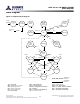
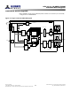
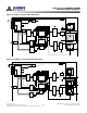
Table Of Contents
- DDR3L SDRAM
- Description
- State Diagram
- Functional Description
- Functional Block Diagrams
- Ball Assignments and Descriptions
- Package Dimensions
- Electrical Specifications
- Thermal Characteristics
- Electrical Specifications – I DD Specifications and Conditions
- Electrical Characteristics – 1.35V IDD Specifications
- Electrical Specifications – DC and AC
- ODT Characteristics
- Output Driver Impedance
- Output Characteristics and Operating Conditions
- Speed Bin Tables
- Electrical Characteristics and AC Operating Conditions
- Electrical Characteristics and AC Operating Conditions
- Command and Address Setup, Hold, and Derating
- Data Setup, Hold, and Derating
- Commands – Truth Tables
- Commands
- Input Clock Frequency Change
- Write Leveling
- Initialization
- Voltage Initialization / Change
- Mode Registers
- Mode Register 0 (MR0)
- Mode Register 1 (MR1)
- Mode Register 2 (MR2)
- Mode Register 3 (MR3)
- MODE REGISTER SET (MRS) Command
- ZQ CALIBRATION Operation
- ACTIVATE Operation
- READ Operation
- WRITE Operation
- PRECHARGE Operation
- SELF REFRESH Operation
- Extended Temperature Usage
- Power-Down Mode
- RESET Operation
- On-Die Termination (ODT)
- Dynamic ODT
- Synchronous ODT Mode
- Asynchronous ODT Mode
- Asynchronous to Synchronous ODT Mode Transition (Power-Down Exit)

• Complete functionality may be described throughout the document; any page or dia-
gram may have been simplified to convey a topic and may not be inclusive of all re-
quirements.
• Any specific requirement takes precedence over a general statement.
• Any functionality not specifically stated is considered undefined, illegal, and not sup-
ported, and can result in unknown operation.
• Row addressing is denoted as A[n:0]. For example, 1Gb: n = 12 (x16); 1Gb: n = 13 (x4,
x8); 2Gb: n = 13 (x16) and 2Gb: n = 14 (x4, x8); 4Gb: n = 14 (x16); and 4Gb: n = 15 (x4,
x8).
• Dynamic ODT has a special use case: when DDR3 devices are architected for use in a
single rank memory array, the ODT ball can be wired HIGH rather than routed. Refer
to the Dynamic ODT Special Use Case section.
• A x16 device's DQ bus is comprised of two bytes. If only one of the bytes needs to be
used, use the lower byte for data transfers and terminate the upper byte as noted:
– Connect UDQS to ground via 1kΩ* resistor.
– Connect UDQS# to V
DD
via 1kΩ* resistor.
– Connect UDM to V
DD
via 1kΩ* resistor.
– Connect DQ[15:8] individually to either V
SS
, V
DD
, or V
REF
via 1kΩ resistors,* or float
DQ[15:8].
*If ODT is used, 1kΩ resistor should be changed to 4x that of the selected ODT.
8Gb: x4, x8, x16 DDR3L SDRAM
Functional Description
13
Rev 2.0 June 2016
© 2015 Alliance Memory, Inc. All rights reserved.
Alliance Memory Inc. reserves the right to change products or specification without notice
Alliance Memory Inc. 511 Taylor Way, San Carlos, CA 94070
TEL: (650) 610-6800 FAX: (650) 620-9211