
Datasheet
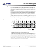
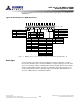

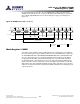
Table Of Contents
- DDR3L SDRAM
- Description
- State Diagram
- Functional Description
- Functional Block Diagrams
- Ball Assignments and Descriptions
- Package Dimensions
- Electrical Specifications
- Thermal Characteristics
- Electrical Specifications – I DD Specifications and Conditions
- Electrical Characteristics – 1.35V IDD Specifications
- Electrical Specifications – DC and AC
- ODT Characteristics
- Output Driver Impedance
- Output Characteristics and Operating Conditions
- Speed Bin Tables
- Electrical Characteristics and AC Operating Conditions
- Electrical Characteristics and AC Operating Conditions
- Command and Address Setup, Hold, and Derating
- Data Setup, Hold, and Derating
- Commands – Truth Tables
- Commands
- Input Clock Frequency Change
- Write Leveling
- Initialization
- Voltage Initialization / Change
- Mode Registers
- Mode Register 0 (MR0)
- Mode Register 1 (MR1)
- Mode Register 2 (MR2)
- Mode Register 3 (MR3)
- MODE REGISTER SET (MRS) Command
- ZQ CALIBRATION Operation
- ACTIVATE Operation
- READ Operation
- WRITE Operation
- PRECHARGE Operation
- SELF REFRESH Operation
- Extended Temperature Usage
- Power-Down Mode
- RESET Operation
- On-Die Termination (ODT)
- Dynamic ODT
- Synchronous ODT Mode
- Asynchronous ODT Mode
- Asynchronous to Synchronous ODT Mode Transition (Power-Down Exit)
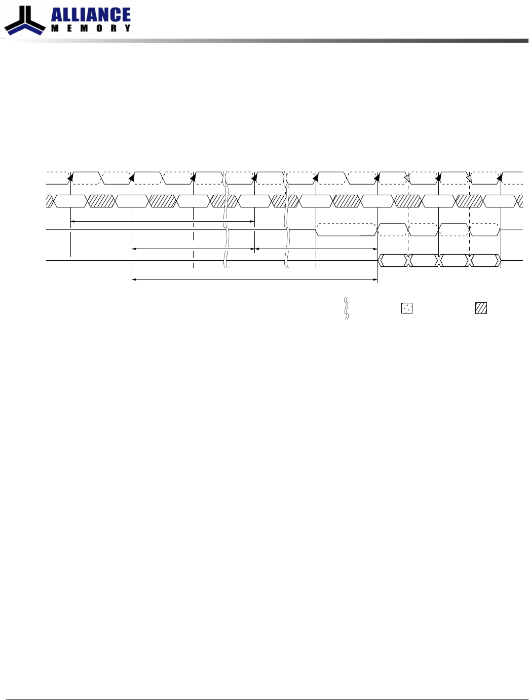
the AL and CAS latency (CL), RL = AL + CL. WRITE latency (WL) is the sum of CAS
WRITE latency and AL, WL = AL + CWL (see Mode Register 2 (MR2) (page 138)). Exam-
ples of READ and WRITE latencies are shown in Figure 53 (page 138) and Figure 55
(page 139).
Figure 53: READ Latency (AL = 5, CL = 6)
CK
CK#
Command
DQ
DQS, DQS#
ACTIVE n
T0 T1
Don’t Care
NOP NOP
T6 T12
NOPREAD n
T13
NOP
DO
n + 3
DO
n + 2
DO
n + 1
RL = AL + CL = 11
T14
NOP
DO
n
t
RCD (MIN)
AL = 5 CL = 6
T11
BC4
Indicates break
in time scale
Transitioning Data
T2
NOP
Mode Register 2 (MR2)
The mode register 2 (MR2) controls additional functions and features not available in
the other mode registers. These additional functions are CAS WRITE latency (CWL), AU-
TO SELF REFRESH (ASR), SELF REFRESH TEMPERATURE (SRT), and DYNAMIC ODT
(R
TT(WR)
). These functions are controlled via the bits shown in Figure 54. The MR2 is
programmed via the MRS command and will retain the stored information until it is
programmed again or until the device loses power. Reprogramming the MR2 register
will not alter the contents of the memory array, provided it is performed correctly. The
MR2 register must be loaded when all banks are idle and no data bursts are in progress,
and the controller must wait the specified time
t
MRD and
t
MOD before initiating a sub-
sequent operation.
8Gb: x4, x8, x16 DDR3L SDRAM
Mode Register 2 (MR2)
138
Rev 2.0 June 2016
© 2015 Alliance Memory, Inc. All rights reserved.
Alliance Memory Inc. reserves the right to change products or specification without notice
Alliance Memory Inc. 511 Taylor Way, San Carlos, CA 94070
TEL: (650) 610-6800 FAX: (650) 620-9211