
Datasheet
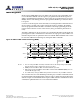

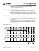
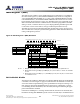
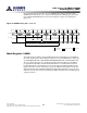
Table Of Contents
- DDR3L SDRAM
- Description
- State Diagram
- Functional Description
- Functional Block Diagrams
- Ball Assignments and Descriptions
- Package Dimensions
- Electrical Specifications
- Thermal Characteristics
- Electrical Specifications – I DD Specifications and Conditions
- Electrical Characteristics – 1.35V IDD Specifications
- Electrical Specifications – DC and AC
- ODT Characteristics
- Output Driver Impedance
- Output Characteristics and Operating Conditions
- Speed Bin Tables
- Electrical Characteristics and AC Operating Conditions
- Electrical Characteristics and AC Operating Conditions
- Command and Address Setup, Hold, and Derating
- Data Setup, Hold, and Derating
- Commands – Truth Tables
- Commands
- Input Clock Frequency Change
- Write Leveling
- Initialization
- Voltage Initialization / Change
- Mode Registers
- Mode Register 0 (MR0)
- Mode Register 1 (MR1)
- Mode Register 2 (MR2)
- Mode Register 3 (MR3)
- MODE REGISTER SET (MRS) Command
- ZQ CALIBRATION Operation
- ACTIVATE Operation
- READ Operation
- WRITE Operation
- PRECHARGE Operation
- SELF REFRESH Operation
- Extended Temperature Usage
- Power-Down Mode
- RESET Operation
- On-Die Termination (ODT)
- Dynamic ODT
- Synchronous ODT Mode
- Asynchronous ODT Mode
- Asynchronous to Synchronous ODT Mode Transition (Power-Down Exit)

vided, and the TDQS# ball is not used. The TDQS function is available in the x8 DDR3
SDRAM configuration only and must be disabled via the mode register for the x4 and
x16 configurations.
On-Die Termination
ODT resistance R
TT,nom
is defined by MR1[9, 6, 2] (see Figure 52 (page 135)). The R
TT
termination value applies to the DQ, DM, DQS, DQS#, and TDQS, TDQS# balls. DDR3
supports multiple R
TT
termination values based on RZQ/n where n can be 2, 4, 6, 8, or
12 and RZQ is 240Ω
Unlike DDR2, DDR3 ODT must be turned off prior to reading data out and must remain
off during a READ burst. R
TT,nom
termination is allowed any time after the DRAM is ini-
tialized, calibrated, and not performing read access, or when it is not in self refresh
mode. Additionally, write accesses with dynamic ODT (R
TT(WR)
) enabled temporarily re-
places R
TT,nom
with R
TT(WR)
.
The actual effective termination, R
TT(EFF)
, may be different from the R
TT
targeted due to
nonlinearity of the termination. For R
TT(EFF)
values and calculations (see On-Die Termi-
nation (ODT) (page 187)).
The ODT feature is designed to improve signal integrity of the memory channel by ena-
bling the DDR3 SDRAM controller to independently turn on/off ODT for any or all devi-
ces. The ODT input control pin is used to determine when R
TT
is turned on (ODTL on)
and off (ODTL off), assuming ODT has been enabled via MR1[9, 6, 2].
Timings for ODT are detailed in On-Die Termination (ODT) (page 187).
WRITE LEVELING
The WRITE LEVELING function is enabled by MR1[7], as shown in Figure 52 (page 135).
Write leveling is used (during initialization) to deskew the DQS strobe to clock offset as
a result of fly-by topology designs. For better signal integrity, DDR3 SDRAM memory
modules adopted fly-by topology for the commands, addresses, control signals, and
clocks.
The fly-by topology benefits from a reduced number of stubs and their lengths. Howev-
er, fly-by topology induces flight time skews between the clock and DQS strobe (and
DQ) at each DRAM on the DIMM. Controllers will have a difficult time maintaining
t
DQSS,
t
DSS, and
t
DSH specifications without supporting write leveling in systems
which use fly-by topology-based modules. Write leveling timing and detailed operation
information is provided in Write Leveling (page 121).
POSTED CAS ADDITIVE Latency
POSTED CAS ADDITIVE latency (AL) is supported to make the command and data bus
efficient for sustainable bandwidths in DDR3 SDRAM. MR1[4, 3] define the value of AL,
as shown in Figure 53 (page 138). MR1[4, 3] enable the user to program the DDR3
SDRAM with AL = 0, CL - 1, or CL - 2.
With this feature, the DDR3 SDRAM enables a READ or WRITE command to be issued
after the ACTIVATE command for that bank prior to
t
RCD (MIN). The only restriction is
ACTIVATE to READ or WRITE + AL ≥
t
RCD (MIN) must be satisfied. Assuming
t
RCD
(MIN) = CL, a typical application using this feature sets AL = CL - 1
t
CK =
t
RCD (MIN) - 1
t
CK. The READ or WRITE command is held for the time of the AL before it is released
internally to the DDR3 SDRAM device. READ latency (RL) is controlled by the sum of
8Gb: x4, x8, x16 DDR3L SDRAM
Mode Register 1 (MR1)
137
Rev 2.0 June 2016
© 2015 Alliance Memory, Inc. All rights reserved.
Alliance Memory Inc. reserves the right to change products or specification without notice
Alliance Memory Inc. 511 Taylor Way, San Carlos, CA 94070
TEL: (650) 610-6800 FAX: (650) 620-9211