
Datasheet
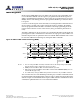

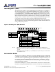
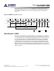
Table Of Contents
- DDR3L SDRAM
- Description
- State Diagram
- Functional Description
- Functional Block Diagrams
- Ball Assignments and Descriptions
- Package Dimensions
- Electrical Specifications
- Thermal Characteristics
- Electrical Specifications – I DD Specifications and Conditions
- Electrical Characteristics – 1.35V IDD Specifications
- Electrical Specifications – DC and AC
- ODT Characteristics
- Output Driver Impedance
- Output Characteristics and Operating Conditions
- Speed Bin Tables
- Electrical Characteristics and AC Operating Conditions
- Electrical Characteristics and AC Operating Conditions
- Command and Address Setup, Hold, and Derating
- Data Setup, Hold, and Derating
- Commands – Truth Tables
- Commands
- Input Clock Frequency Change
- Write Leveling
- Initialization
- Voltage Initialization / Change
- Mode Registers
- Mode Register 0 (MR0)
- Mode Register 1 (MR1)
- Mode Register 2 (MR2)
- Mode Register 3 (MR3)
- MODE REGISTER SET (MRS) Command
- ZQ CALIBRATION Operation
- ACTIVATE Operation
- READ Operation
- WRITE Operation
- PRECHARGE Operation
- SELF REFRESH Operation
- Extended Temperature Usage
- Power-Down Mode
- RESET Operation
- On-Die Termination (ODT)
- Dynamic ODT
- Synchronous ODT Mode
- Asynchronous ODT Mode
- Asynchronous to Synchronous ODT Mode Transition (Power-Down Exit)

upon exit of SELF REFRESH operation. If the DLL is disabled prior to entering self re-
fresh mode, the DLL remains disabled even upon exit of SELF REFRESH operation until
it is re-enabled and reset.
The DRAM is not tested to check—nor does Alliance Memory warrant compliance with
—normal mode
timings or functionality when the DLL is disabled. An attempt has
been made to have the DRAM operate in the normal mode where reasonably possible
when the DLL has been disabled; however, by industry standard, a few known
exceptions are defined:
• ODT is not allowed to be used
• The output data is no longer edge-aligned to the clock
• CL and CWL can only be six clocks
When the DLL is disabled, timing and functionality can vary from the normal operation
specifications when the DLL is enabled (see DLL Disable Mode (page 115)). Disabling
the DLL also implies the need to change the clock frequency (see Input Clock Frequen-
cy Change (page 119)).
Output Drive Strength
The DDR3 SDRAM uses a programmable impedance output buffer. The drive strength
mode register setting is defined by MR1[5, 1]. RZQ/7 (34Ω [NOM]) is the primary output
driver impedance setting for DDR3 SDRAM devices. To calibrate the output driver im-
pedance, an external precision resistor (RZQ) is connected between the ZQ ball and
V
SSQ
. The value of the resistor must be 240Ω
The output impedance is set during initialization. Additional impedance calibration up-
dates do not affect device operation, and all data sheet timings and current specifica-
tions are met during an update.
To meet the 34Ω specification, the output drive strength must be set to 34Ω during initi-
alization. To obtain a calibrated output driver impedance after power-up, the DDR3
SDRAM needs a calibration command that is part of the initialization and reset proce-
dure.
OUTPUT ENABLE/DISABLE
The OUTPUT ENABLE function is defined by MR1[12], as shown in Figure 52
(page 135). When enabled (MR1[12] = 0), all outputs (DQ, DQS, DQS#) function when in
the normal mode of operation. When disabled (MR1[12] = 1), all DDR3 SDRAM outputs
(DQ and DQS, DQS#) are tri-stated. The output disable feature is intended to be used
during I
DD
characterization of the READ current and during
t
DQSS margining (write
leveling) only.
TDQS Enable
Termination data strobe (TDQS) is a feature of the x8 DDR3 SDRAM configuration that
provides termination resistance (R
TT
) and may be useful in some system configurations.
TDQS is not supported in x4 or x16 configurations. When enabled via the mode register
(MR1[11]), the R
TT
that is applied to DQS and DQS# is also applied to TDQS and TDQS#.
In contrast to the RDQS function of DDR2 SDRAM, DDR3’s TDQS provides the termina-
tion resistance R
TT
only. The OUTPUT DATA STROBE function of RDQS is not provided
by TDQS; thus, R
ON
does not apply to TDQS and TDQS#. The TDQS and DM functions
share the same ball. When the TDQS function is enabled via the mode register, the DM
function is not supported. When the TDQS function is disabled, the DM function is pro-
8Gb: x4, x8, x16 DDR3L SDRAM
Mode Register 1 (MR1)
136
Rev 2.0 June 2016
© 2015 Alliance Memory, Inc. All rights reserved.
Alliance Memory Inc. reserves the right to change products or specification without notice
Alliance Memory Inc. 511 Taylor Way, San Carlos, CA 94070
TEL: (650) 610-6800 FAX: (650) 620-9211