
Datasheet
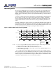

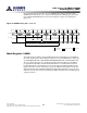
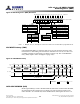
Table Of Contents
- DDR3L SDRAM
- Description
- State Diagram
- Functional Description
- Functional Block Diagrams
- Ball Assignments and Descriptions
- Package Dimensions
- Electrical Specifications
- Thermal Characteristics
- Electrical Specifications – I DD Specifications and Conditions
- Electrical Characteristics – 1.35V IDD Specifications
- Electrical Specifications – DC and AC
- ODT Characteristics
- Output Driver Impedance
- Output Characteristics and Operating Conditions
- Speed Bin Tables
- Electrical Characteristics and AC Operating Conditions
- Electrical Characteristics and AC Operating Conditions
- Command and Address Setup, Hold, and Derating
- Data Setup, Hold, and Derating
- Commands – Truth Tables
- Commands
- Input Clock Frequency Change
- Write Leveling
- Initialization
- Voltage Initialization / Change
- Mode Registers
- Mode Register 0 (MR0)
- Mode Register 1 (MR1)
- Mode Register 2 (MR2)
- Mode Register 3 (MR3)
- MODE REGISTER SET (MRS) Command
- ZQ CALIBRATION Operation
- ACTIVATE Operation
- READ Operation
- WRITE Operation
- PRECHARGE Operation
- SELF REFRESH Operation
- Extended Temperature Usage
- Power-Down Mode
- RESET Operation
- On-Die Termination (ODT)
- Dynamic ODT
- Synchronous ODT Mode
- Asynchronous ODT Mode
- Asynchronous to Synchronous ODT Mode Transition (Power-Down Exit)

Mode Register 1 (MR1)
The mode register 1 (MR1) controls additional functions and features not available in
the other mode registers: Q OFF (OUTPUT DISABLE), TDQS (for the x8 configuration
only), DLL ENABLE/DLL DISABLE, R
TT,nom
value (ODT), WRITE LEVELING, POSTED
CAS ADDITIVE latency, and OUTPUT DRIVE STRENGTH. These functions are control-
led via the bits shown in Figure 52 (page 135). The MR1 register is programmed via the
MRS command and retains the stored information until it is reprogrammed, until RE-
SET# goes LOW, or until the device loses power. Reprogramming the MR1 register will
not alter the contents of the memory array, provided it is performed correctly.
The MR1 register must be loaded when all banks are idle and no bursts are in progress.
The controller must satisfy the specified timing parameters
t
MRD and
t
MOD before ini-
tiating a subsequent operation.
Figure 52: Mode Register 1 (MR1) Definition
AL
R
TT
Q Off
A9 A7 A6 A5 A4 A3A8 A2 A1 A0
Mode register 1 (MR1)
Address bus
9765438210
A10A12 A11BA0BA1
10111213
M0
0
1
DLL Enable
Enable (normal)
Disable
M5
0
0
1
1
Output Drive St rength
RZQ/6 (40Ω [NOM])
RZQ/7 (34Ω [NOM])
Reserved
Reserved
14
WL
0
1
0
1
1
0
ODS DLL
R
TT
TDQS
M12
0
1
Q Off
Enabled
Disabled
BA2
15
0
1
M7
0
1
Write Levelization
Disable (normal)
Enable
Additive Latency (AL)
Disabled (AL = 0)
AL = CL - 1
AL = CL - 2
Reserved
M3
0
1
0
1
M4
0
0
1
1
R
TT
ODS
M1
0
1
0
1
A13A14A15
161718
0
1
M11
0
1
TDQS
Disabled
Enabled
0
1
0
1
R
TT,nom
(ODT)
2
Non- Writes
R
TT,nom
disabled
RZQ/4 (60Ω [NOM])
RZQ/2 (120Ω [NOM])
RZQ/6 (40Ω [NOM])
RZQ/12 (20Ω [NOM])
RZQ/8 (30Ω [NOM])
Reserved
Reserved
R
TT,nom
(ODT)
3
Writes
R
TT,nom
disabled
RZQ/4 (60Ω [NOM])
RZQ/2 (120Ω [NOM])
RZQ/6 (40Ω [NOM])
n/a
n/a
Reserved
Reserved
M2
0
1
0
1
0
1
0
1
M6
0
0
1
1
0
0
1
1
M9
0
0
0
0
1
1
1
1
Mode Register
Mode register set 0 (MR0)
Mode register set 1 (MR1)
Mode register set 2 (MR2)
Mode register set 3 (MR3)
M16
0
1
0
1
M17
0
0
1
1
Notes:
1. MR1[18, 15:13, 10, 8] are reserved for future use and must be programmed to 0.
2. During write leveling, if MR1[7] and MR1[12] are 1, then all R
TT,nom
values are available
for use.
3. During write leveling, if MR1[7] is a 1, but MR1[12] is a 0, then only R
TT,nom
write values
are available for use.
DLL Enable/DLL Disable
The DLL may be enabled or disabled by programming MR1[0] during the LOAD MODE
command, as shown in Figure 52 (page 135). The DLL must be enabled for normal oper-
ation. DLL enable is required during power-up initialization and upon returning to nor-
mal operation after having disabled the DLL for the purpose of debugging or evalua-
tion. Enabling the DLL should always be followed by resetting the DLL using the appro-
priate LOAD MODE command.
If the DLL is enabled prior to entering self refresh mode, the DLL is automatically disa-
bled when entering SELF REFRESH operation and is automatically re-enabled and reset
8Gb: x4, x8, x16 DDR3L SDRAM
Mode Register 1 (MR1)
135
Rev 2.0 June 2016
© 2015 Alliance Memory, Inc. All rights reserved.
Alliance Memory Inc. reserves the right to change products or specification without notice
Alliance Memory Inc. 511 Taylor Way, San Carlos, CA 94070
TEL: (650) 610-6800 FAX: (650) 620-9211