
Datasheet
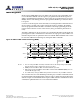

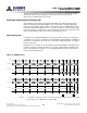
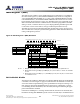
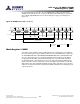
Table Of Contents
- DDR3L SDRAM
- Description
- State Diagram
- Functional Description
- Functional Block Diagrams
- Ball Assignments and Descriptions
- Package Dimensions
- Electrical Specifications
- Thermal Characteristics
- Electrical Specifications – I DD Specifications and Conditions
- Electrical Characteristics – 1.35V IDD Specifications
- Electrical Specifications – DC and AC
- ODT Characteristics
- Output Driver Impedance
- Output Characteristics and Operating Conditions
- Speed Bin Tables
- Electrical Characteristics and AC Operating Conditions
- Electrical Characteristics and AC Operating Conditions
- Command and Address Setup, Hold, and Derating
- Data Setup, Hold, and Derating
- Commands – Truth Tables
- Commands
- Input Clock Frequency Change
- Write Leveling
- Initialization
- Voltage Initialization / Change
- Mode Registers
- Mode Register 0 (MR0)
- Mode Register 1 (MR1)
- Mode Register 2 (MR2)
- Mode Register 3 (MR3)
- MODE REGISTER SET (MRS) Command
- ZQ CALIBRATION Operation
- ACTIVATE Operation
- READ Operation
- WRITE Operation
- PRECHARGE Operation
- SELF REFRESH Operation
- Extended Temperature Usage
- Power-Down Mode
- RESET Operation
- On-Die Termination (ODT)
- Dynamic ODT
- Synchronous ODT Mode
- Asynchronous ODT Mode
- Asynchronous to Synchronous ODT Mode Transition (Power-Down Exit)
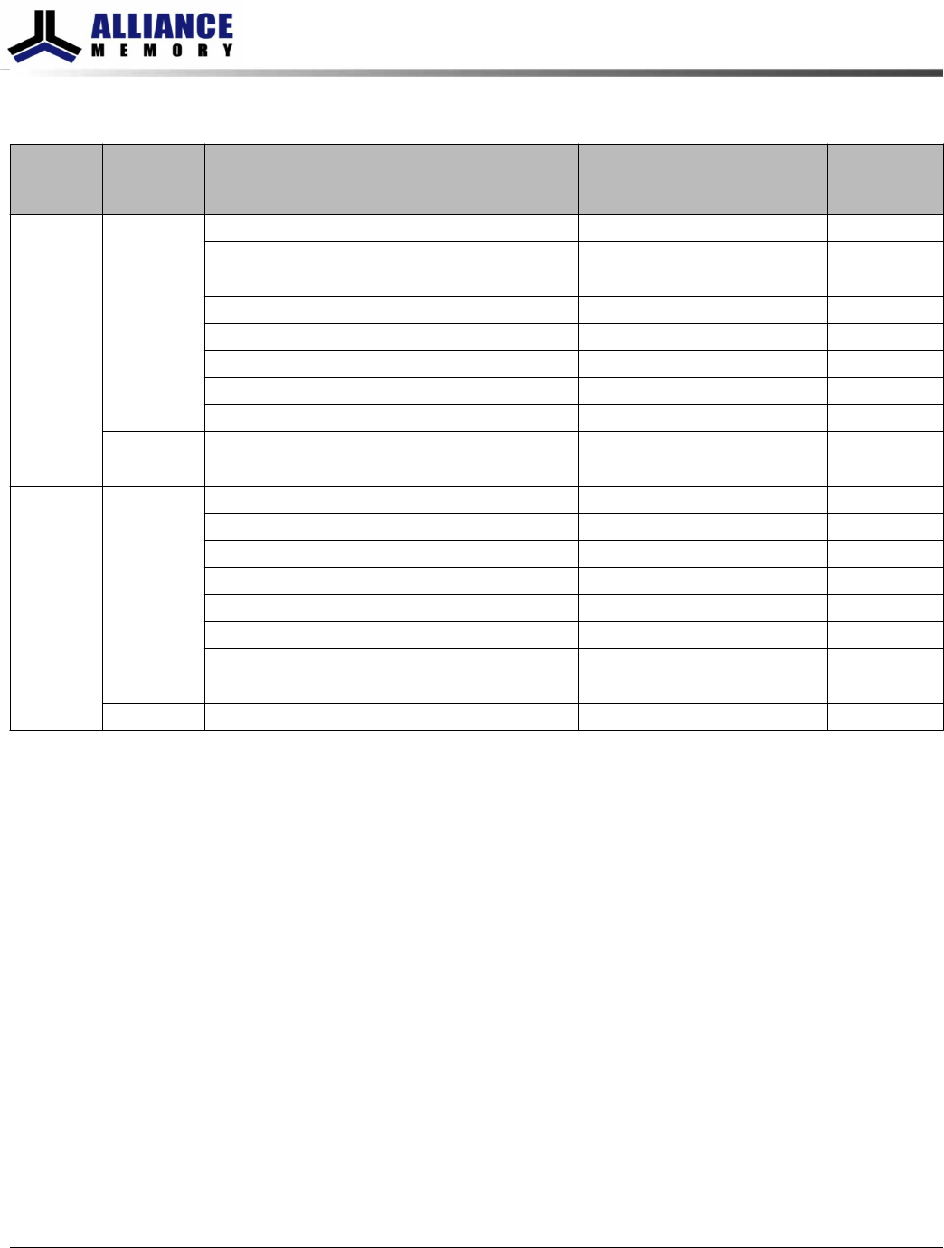
Table 73: Burst Order
Burst
Length
READ/
WRITE
Starting
Column Address
(A[2, 1, 0])
Burst Type = Sequential
(Decimal)
Burst Type = Interleaved
(Decimal)
Notes
4 (chop) READ 0 0 0 0, 1, 2, 3, Z, Z, Z, Z 0, 1, 2, 3, Z, Z, Z, Z 1, 2
0 0 1 1, 2, 3, 0, Z, Z, Z, Z 1, 0, 3, 2, Z, Z, Z, Z 1, 2
0 1 0 2, 3, 0, 1, Z, Z, Z, Z 2, 3, 0, 1, Z, Z, Z, Z 1, 2
0 1 1 3, 0, 1, 2, Z, Z, Z, Z 3, 2, 1, 0, Z, Z, Z, Z 1, 2
1 0 0 4, 5, 6, 7, Z, Z, Z, Z 4, 5, 6, 7, Z, Z, Z, Z 1, 2
1 0 1 5, 6, 7, 4, Z, Z, Z, Z 5, 4, 7, 6, Z, Z, Z, Z 1, 2
1 1 0 6, 7, 4, 5, Z, Z, Z, Z 6, 7, 4, 5, Z, Z, Z, Z 1, 2
1 1 1 7, 4, 5, 6, Z, Z, Z, Z 7, 6, 5, 4, Z, Z, Z, Z 1, 2
WRITE 0 V V 0, 1, 2, 3, X, X, X, X 0, 1, 2, 3, X, X, X, X 1, 3, 4
1 V V 4, 5, 6, 7, X, X, X, X 4, 5, 6, 7, X, X, X, X 1, 3, 4
8 (fixed) READ 0 0 0 0, 1, 2, 3, 4, 5, 6, 7 0, 1, 2, 3, 4, 5, 6, 7 1
0 0 1 1, 2, 3, 0, 5, 6, 7, 4 1, 0, 3, 2, 5, 4, 7, 6 1
0 1 0 2, 3, 0, 1, 6, 7, 4, 5 2, 3, 0, 1, 6, 7, 4, 5 1
0 1 1 3, 0, 1, 2, 7, 4, 5, 6 3, 2, 1, 0, 7, 6, 5, 4 1
1 0 0 4, 5, 6, 7, 0, 1, 2, 3 4, 5, 6, 7, 0, 1, 2, 3 1
1 0 1 5, 6, 7, 4, 1, 2, 3, 0 5, 4, 7, 6, 1, 0, 3, 2 1
1 1 0 6, 7, 4, 5, 2, 3, 0, 1 6, 7, 4, 5, 2, 3, 0, 1 1
1 1 1 7, 4, 5, 6, 3, 0, 1, 2 7, 6, 5, 4, 3, 2, 1, 0 1
WRITE V V V 0, 1, 2, 3, 4, 5, 6, 7 0, 1, 2, 3, 4, 5, 6, 7 1, 3
Notes:
1. Internal READ and WRITE operations start at the same point in time for BC4 as they do
for BL8.
2. Z = Data and strobe output drivers are in tri-state.
3. V = A valid logic level (0 or 1), but the respective input buffer ignores level-on input
pins.
4. X = “Don’t Care.”
DLL RESET
DLL RESET is defined by MR0[8] (see Figure 50 (page 132)). Programming MR0[8] to 1
activates the DLL RESET function. MR0[8] is self-clearing, meaning it returns to a value
of 0 after the DLL RESET function has been initiated.
Anytime the DLL RESET function is initiated, CKE must be HIGH and the clock held
stable for 512 (
t
DLLK) clock cycles before a READ command can be issued. This is to
allow time for the internal clock to be synchronized with the external clock. Failing to
wait for synchronization can result in invalid output timing specifications, such as
t
DQSCK timings.
Write Recovery
WRITE recovery time is defined by MR0[11:9] (see Figure 50 (page 132)). Write recovery
values of 5, 6, 7, 8, 10, or 12 can be used by programming MR0[11:9]. The user is re-
8Gb: x4, x8, x16 DDR3L SDRAM
Mode Register 0 (MR0)
133
Rev 2.0 June 2016
© 2015 Alliance Memory, Inc. All rights reserved.
Alliance Memory Inc. reserves the right to change products or specification without notice
Alliance Memory Inc. 511 Taylor Way, San Carlos, CA 94070
TEL: (650) 610-6800 FAX: (650) 620-9211