
Datasheet
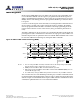

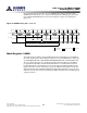
Table Of Contents
- DDR3L SDRAM
- Description
- State Diagram
- Functional Description
- Functional Block Diagrams
- Ball Assignments and Descriptions
- Package Dimensions
- Electrical Specifications
- Thermal Characteristics
- Electrical Specifications – I DD Specifications and Conditions
- Electrical Characteristics – 1.35V IDD Specifications
- Electrical Specifications – DC and AC
- ODT Characteristics
- Output Driver Impedance
- Output Characteristics and Operating Conditions
- Speed Bin Tables
- Electrical Characteristics and AC Operating Conditions
- Electrical Characteristics and AC Operating Conditions
- Command and Address Setup, Hold, and Derating
- Data Setup, Hold, and Derating
- Commands – Truth Tables
- Commands
- Input Clock Frequency Change
- Write Leveling
- Initialization
- Voltage Initialization / Change
- Mode Registers
- Mode Register 0 (MR0)
- Mode Register 1 (MR1)
- Mode Register 2 (MR2)
- Mode Register 3 (MR3)
- MODE REGISTER SET (MRS) Command
- ZQ CALIBRATION Operation
- ACTIVATE Operation
- READ Operation
- WRITE Operation
- PRECHARGE Operation
- SELF REFRESH Operation
- Extended Temperature Usage
- Power-Down Mode
- RESET Operation
- On-Die Termination (ODT)
- Dynamic ODT
- Synchronous ODT Mode
- Asynchronous ODT Mode
- Asynchronous to Synchronous ODT Mode Transition (Power-Down Exit)
ing location within the block. The programmed burst length applies to both READ and
WRITE bursts.
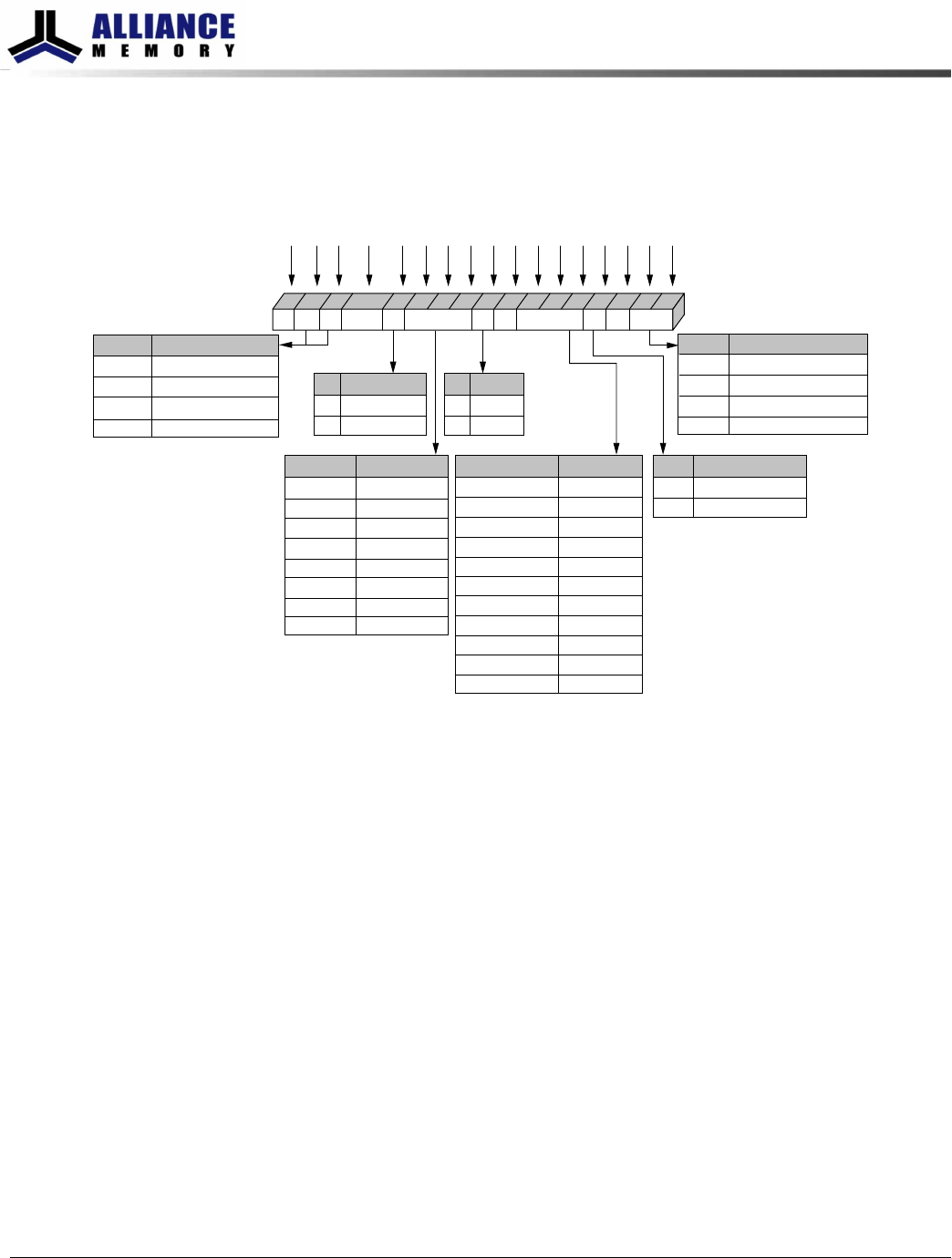
Figure 50: Mode Register 0 (MR0) Definitions
BL
CAS# latency CLBTPD
A9 A7 A6 A5 A4 A3A8 A2 A1 A0
Mode register 0 (MR0)
Address bus
9765438210
A10A12 A11BA0BA1
10111215–13
M3
0
1
READ Burst Type
Sequential (nibble)
Interleaved
CAS Latency
Reserved
5
6
7
8
9
10
11
12
13
14
M2
0
0
0
0
0
0
0
0
1
1
1
M4
0
1
0
1
0
1
0
1
0
1
0
M5
0
0
1
1
0
0
1
1
0
0
1
M6
0
0
0
0
1
1
1
1
0
0
0
17
DLL
Write Recovery
16
5
6
7
8
10
12
14
WR00
M12
0
1
Precharge PD
DLL off
(slow exit)
DLL on
(fast exit)
BA2
18
0
1
Burst Length
Fixed BL8
4 or 8 (on-the-fly via A12)
Fixed BC4 (chop)
Reserved
M0
0
1
0
1
M1
0
0
1
1
M9
0
1
0
1
0
1
0
1
M10
0
0
1
1
0
0
1
1
M11
0
0
0
0
1
1
1
1
M14
0
1
0
1
M15
0
0
1
1
Mode Register
Mode register 0 (MR0)
Mode register 1 (MR1)
Mode register 2 (MR2)
Mode register 3 (MR3)
A[15:13]
16
0
1
0
1
M8
0
1
DLL Reset
No
Yes
Note:
1. MR0[18, 15:13, 7] are reserved for future use and must be programmed to 0.
Burst Type
Accesses within a given burst can be programmed to either a sequential or an inter-
leaved order. The burst type is selected via MR0[3] (see Figure 50 (page 132)). The order-
ing of accesses within a burst is determined by the burst length, the burst type, and the
starting column address. DDR3 only supports 4-bit burst chop and 8-bit burst access
modes. Full interleave address ordering is supported for READs, while WRITEs are re-
stricted to nibble (BC4) or word (BL8) boundaries.
8Gb: x4, x8, x16 DDR3L SDRAM
Mode Register 0 (MR0)
132
Rev 2.0 June 2016
© 2015 Alliance Memory, Inc. All rights reserved.
Alliance Memory Inc. reserves the right to change products or specification without notice
Alliance Memory Inc. 511 Taylor Way, San Carlos, CA 94070
TEL: (650) 610-6800 FAX: (650) 620-9211