
Datasheet
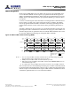

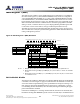
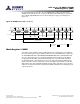
Table Of Contents
- DDR3L SDRAM
- Description
- State Diagram
- Functional Description
- Functional Block Diagrams
- Ball Assignments and Descriptions
- Package Dimensions
- Electrical Specifications
- Thermal Characteristics
- Electrical Specifications – I DD Specifications and Conditions
- Electrical Characteristics – 1.35V IDD Specifications
- Electrical Specifications – DC and AC
- ODT Characteristics
- Output Driver Impedance
- Output Characteristics and Operating Conditions
- Speed Bin Tables
- Electrical Characteristics and AC Operating Conditions
- Electrical Characteristics and AC Operating Conditions
- Command and Address Setup, Hold, and Derating
- Data Setup, Hold, and Derating
- Commands – Truth Tables
- Commands
- Input Clock Frequency Change
- Write Leveling
- Initialization
- Voltage Initialization / Change
- Mode Registers
- Mode Register 0 (MR0)
- Mode Register 1 (MR1)
- Mode Register 2 (MR2)
- Mode Register 3 (MR3)
- MODE REGISTER SET (MRS) Command
- ZQ CALIBRATION Operation
- ACTIVATE Operation
- READ Operation
- WRITE Operation
- PRECHARGE Operation
- SELF REFRESH Operation
- Extended Temperature Usage
- Power-Down Mode
- RESET Operation
- On-Die Termination (ODT)
- Dynamic ODT
- Synchronous ODT Mode
- Asynchronous ODT Mode
- Asynchronous to Synchronous ODT Mode Transition (Power-Down Exit)
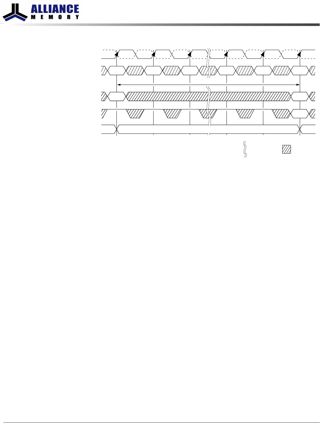
Figure 49: MRS to nonMRS Command Timing (
t
MOD)
Valid Valid
MRS
non
MRS
NOP NOP NOP NOP
T0 T1 T2 Ta0 Ta1 Ta2
CK#
CK
Command
Address
CKE
Valid
Old
setting
New
setting
Indicates break
in time scale
t
MOD
Updating setting
Don’t Care
Notes:
1. Prior to issuing the MRS command, all banks must be idle (they must be precharged,
t
RP
must be satisfied, and no data bursts can be in progress).
2. Prior to Ta2 when
t
MOD (MIN) is being satisfied, no commands (except NOP/DES) may be
issued.
3. If R
TT
was previously enabled, ODT must be registered LOW at T0 so that ODTL is satis-
fied prior to Ta1. ODT must also be registered LOW at each rising CK edge from T0 until
t
MODmin is satisfied at Ta2.
4. CKE must be registered HIGH from the MRS command until
t
MRSPDEN (MIN), at which
time power-down may occur (see Power-Down Mode (page 177)).
Mode Register 0 (MR0)
The base register, mode register 0 (MR0), is used to define various DDR3 SDRAM modes
of operation. These definitions include the selection of a burst length, burst type, CAS
latency, operating mode, DLL RESET, write recovery, and precharge power-down mode
(see Figure 50 (page 132)).
Burst Length
Burst length is defined by MR0[1:0]. Read and write accesses to the DDR3 SDRAM are
burst-oriented, with the burst length being programmable to 4 (chop) mode, 8 (fixed)
mode, or selectable using A12 during a READ/WRITE command (on-the-fly). The burst
length determines the maximum number of column locations that can be accessed for
a given READ or WRITE command. When MR0[1:0] is set to 01 during a READ/WRITE
command, if A12 = 0, then BC4 mode is selected. If A12 = 1, then BL8 mode is selected.
Specific timing diagrams, and turnaround between READ/WRITE, are shown in the
READ/WRITE sections of this document.
When a READ or WRITE command is issued, a block of columns equal to the burst
length is effectively selected. All accesses for that burst take place within this block,
meaning that the burst will wrap within the block if a boundary is reached. The block is
uniquely selected by A[i:2] when the burst length is set to 4 and by A[i:3] when the burst
length is set to 8, where Ai is the most significant column address bit for a given config-
uration. The remaining (least significant) address bit(s) is (are) used to select the start-
8Gb: x4, x8, x16 DDR3L SDRAM
Mode Register 0 (MR0)
131
Rev 2.0 June 2016
© 2015 Alliance Memory, Inc. All rights reserved.
Alliance Memory Inc. reserves the right to change products or specification without notice
Alliance Memory Inc. 511 Taylor Way, San Carlos, CA 94070
TEL: (650) 610-6800 FAX: (650) 620-9211