
Datasheet
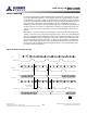
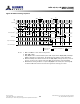

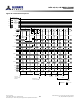
Table Of Contents
- DDR3L SDRAM
- Description
- State Diagram
- Functional Description
- Functional Block Diagrams
- Ball Assignments and Descriptions
- Package Dimensions
- Electrical Specifications
- Thermal Characteristics
- Electrical Specifications – I DD Specifications and Conditions
- Electrical Characteristics – 1.35V IDD Specifications
- Electrical Specifications – DC and AC
- ODT Characteristics
- Output Driver Impedance
- Output Characteristics and Operating Conditions
- Speed Bin Tables
- Electrical Characteristics and AC Operating Conditions
- Electrical Characteristics and AC Operating Conditions
- Command and Address Setup, Hold, and Derating
- Data Setup, Hold, and Derating
- Commands – Truth Tables
- Commands
- Input Clock Frequency Change
- Write Leveling
- Initialization
- Voltage Initialization / Change
- Mode Registers
- Mode Register 0 (MR0)
- Mode Register 1 (MR1)
- Mode Register 2 (MR2)
- Mode Register 3 (MR3)
- MODE REGISTER SET (MRS) Command
- ZQ CALIBRATION Operation
- ACTIVATE Operation
- READ Operation
- WRITE Operation
- PRECHARGE Operation
- SELF REFRESH Operation
- Extended Temperature Usage
- Power-Down Mode
- RESET Operation
- On-Die Termination (ODT)
- Dynamic ODT
- Synchronous ODT Mode
- Asynchronous ODT Mode
- Asynchronous to Synchronous ODT Mode Transition (Power-Down Exit)
V
DD
Voltage Switching
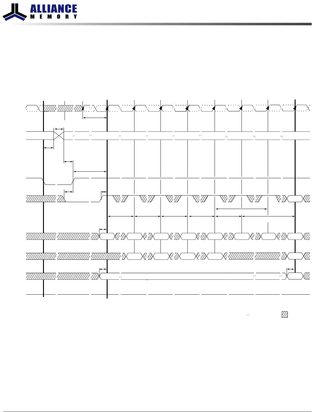
After the DDR3L DRAM is powered up and initialized, the power supply can be altered
between the DDR3L and DDR3 levels, provided the sequence in Figure 47 is main-
tained.
Figure 47: V
DD
Voltage Switching
(
)
(
)
(
)
(
)
CKE
R
TT
BA
(
)
(
)
(
)
(
)
CK, CK#
Command
Note 1 Note 1
(
)
(
)
(
)
(
)
TdTc
Tg
Don’t Care
(
)
(
)
(
)
(
)
(
)
(
)
t
IS
ODT
(
)
(
)
(
)
(
)
Th
t
MRD
t
MOD
(
)
(
)
(
)
(
)
MRSMRS
(
)
(
)
(
)
(
)
(
)
(
)
(
)
(
)
(
)
(
)
(
)
(
)
(
)
(
)
(
)
(
)
(
)
(
)
(
)
(
)
(
)
(
)
(
)
(
)
t
MRD
t
MRD
(
)
(
)
(
)
(
)
(
)
(
)
(
)
(
)
MRS
MR0MR1
MR3
MRS
MR2
(
)
(
)
(
)
(
)
(
)
(
)
(
)
(
)
(
)
(
)
(
)
(
)
Ti Tj Tk
(
)
(
)
(
)
(
)
RESET#
(
)
(
)
(
)
(
)
(
)
(
)
(
)
(
)
(
)
(
)
T = 500μs
(
)
(
)
(
)
(
)
(
)
(
)
Te
Ta
Tb Tf
(
)
(
)
(
)
(
)
ZQCL
(
)
(
)
(
)
(
)
(
)
(
)
(
)
(
)
(
)
(
)
(
)
(
)
(
)
(
)
(
)
(
)
(
)
(
)
(
)
(
)
t
IS
Static LOW in case R
TT,nom
is enabled at time Tg, otherwise static HIGH or LOW
(
)
(
)
(
)
(
)
(
)
(
)
(
)
(
)
t
IS
t
IS
t
XPR
(
)
(
)
(
)
(
)
(
)
(
)
(
)
(
)
(
)
(
)
(
)
(
)
Time break
T
MIN
= 10ns
T
MIN
= 10ns
T
MIN
= 10ns
T
MIN
= 200μs
t
CKSRX
V
DD
, V
DDQ
(DDR3)
(
)
(
)
(
)
(
)
t
DLLK
(
)
(
)
(
)
(
)
(
)
(
)
(
)
(
)
t
ZQinit
(
)
(
)
(
)
(
)
(
)
(
)
(
)
(
)
(
)
(
)
(
)
(
)
(
)
(
)
(
)
(
)
(
)
(
)
(
)
(
)
(
)
(
)
(
)
(
)
(
)
(
)
(
)
(
)
(
)
(
)
(
)
(
)
(
)
(
)
(
)
(
)
(
)
(
)
(
)
(
)
(
)
(
)
V
DD
, V
DDQ
(DDR3L)
(
)
(
)
(
)
(
)
(
)
(
)
(
)
(
)
(
)
(
)
(
)
(
)
(
)
(
)
(
)
(
)
(
)
(
)
(
)
(
)
(
)
(
)
(
)
(
)
(
)
(
)
(
)
(
)
(
)
(
)
(
)
(
)
(
)
(
)
(
)
(
)
(
)
(
)
(
)
(
)
(
)
(
)
(
)
(
)
(
)
(
)
(
)
(
)
(
)
(
)
(
)
(
)
Valid
Valid
Valid
Valid
(
)
(
)
(
)
(
)
(
)
(
)
(
)
(
)
(
)
(
)
(
)
(
)
(
)
(
)
(
)
(
)
(
)
(
)
(
)
(
)
(
)
(
)
Note:
1. From time point Td until Tk, NOP or DES commands must be applied between MRS and
ZQCL commands.
8Gb: x4, x8, x16 DDR3L SDRAM
Voltage Initialization / Change
129
Rev 2.0 June 2016
© 2015 Alliance Memory, Inc. All rights reserved.
Alliance Memory Inc. reserves the right to change products or specification without notice
Alliance Memory Inc. 511 Taylor Way, San Carlos, CA 94070
TEL: (650) 610-6800 FAX: (650) 620-9211