
Datasheet
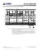
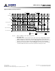

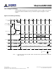
Table Of Contents
- DDR3L SDRAM
- Description
- State Diagram
- Functional Description
- Functional Block Diagrams
- Ball Assignments and Descriptions
- Package Dimensions
- Electrical Specifications
- Thermal Characteristics
- Electrical Specifications – I DD Specifications and Conditions
- Electrical Characteristics – 1.35V IDD Specifications
- Electrical Specifications – DC and AC
- ODT Characteristics
- Output Driver Impedance
- Output Characteristics and Operating Conditions
- Speed Bin Tables
- Electrical Characteristics and AC Operating Conditions
- Electrical Characteristics and AC Operating Conditions
- Command and Address Setup, Hold, and Derating
- Data Setup, Hold, and Derating
- Commands – Truth Tables
- Commands
- Input Clock Frequency Change
- Write Leveling
- Initialization
- Voltage Initialization / Change
- Mode Registers
- Mode Register 0 (MR0)
- Mode Register 1 (MR1)
- Mode Register 2 (MR2)
- Mode Register 3 (MR3)
- MODE REGISTER SET (MRS) Command
- ZQ CALIBRATION Operation
- ACTIVATE Operation
- READ Operation
- WRITE Operation
- PRECHARGE Operation
- SELF REFRESH Operation
- Extended Temperature Usage
- Power-Down Mode
- RESET Operation
- On-Die Termination (ODT)
- Dynamic ODT
- Synchronous ODT Mode
- Asynchronous ODT Mode
- Asynchronous to Synchronous ODT Mode Transition (Power-Down Exit)

Initialization
The following sequence is required for power-up and initialization, as shown in Fig-
ure 46 (page 127):
1. Apply power. RESET# is recommended to be below 0.2 × V
DDQ
during power ramp
to ensure the outputs remain disabled (High-Z) and ODT off (R
TT
is also High-Z).
All other inputs, including ODT, may be undefined.
During power-up, either of the following conditions may exist and must be met:
• Condition A:
–V
DD
and V
DDQ
are driven from a single-power converter output and are
ramped with a maximum delta voltage between them of ΔV ≤ 300mV. Slope re-
versal of any power supply signal is allowed. The voltage levels on all balls oth-
er than V
DD
, V
DDQ
, V
SS
, V
SSQ
must be less than or equal to V
DDQ
and V
DD
on
one side, and must be greater than or equal to V
SSQ
and V
SS
on the other side.
– Both V
DD
and V
DDQ
power supplies ramp to V
DD,min
and V
DDQ,min
within
t
V
DDPR
= 200ms.
–V
REFDQ
tracks V
DD
× 0.5, V
REFCA
tracks V
DD
× 0.5.
–V
TT
is limited to 0.95V when the power ramp is complete and is not applied
directly to the device; however,
t
VTD should be greater than or equal to 0 to
avoid device latchup.
• Condition B:
–V
DD
may be applied before or at the same time as V
DDQ
.
–V
DDQ
may be applied before or at the same time as V
TT
, V
REFDQ
, and V
REFCA
.
– No slope reversals are allowed in the power supply ramp for this condition.
2. Until stable power, maintain RESET# LOW to ensure the outputs remain disabled
(High-Z). After the power is stable, RESET# must be LOW for at least 200μs to be-
gin the initialization process. ODT will remain in the High-Z state while RESET# is
LOW and until CKE is registered HIGH.
3. CKE must be LOW 10ns prior to RESET# transitioning HIGH.
4. After RESET# transitions HIGH, wait 500μs (minus one clock) with CKE LOW.
5. After the CKE LOW time, CKE may be brought HIGH (synchronously) and only
NOP or DES commands may be issued. The clock must be present and valid for at
least 10ns (and a minimum of five clocks) and ODT must be driven LOW at least
t
IS prior to CKE being registered HIGH. When CKE is registered HIGH, it must be
continuously registered HIGH until the full initialization process is complete.
6. After CKE is registered HIGH and after
t
XPR has been satisfied, MRS commands
may be issued. Issue an MRS (LOAD MODE) command to MR2 with the applicable
settings (provide LOW to BA2 and BA0 and HIGH to BA1).
7. Issue an MRS command to MR3 with the applicable settings.
8. Issue an MRS command to MR1 with the applicable settings, including enabling
the DLL and configuring ODT.
9. Issue an MRS command to MR0 with the applicable settings, including a DLL RE-
SET command.
t
DLLK (512) cycles of clock input are required to lock the DLL.
10. Issue a ZQCL command to calibrate R
TT
and R
ON
values for the process voltage
temperature (PVT). Prior to normal operation,
t
ZQinit must be satisfied.
11. When
t
DLLK and
t
ZQinit have been satisfied, the DDR3 SDRAM will be ready for
normal operation.
8Gb: x4, x8, x16 DDR3L SDRAM
Initialization
126
Rev 2.0 June 2016
© 2015 Alliance Memory, Inc. All rights reserved.
Alliance Memory Inc. reserves the right to change products or specification without notice
Alliance Memory Inc. 511 Taylor Way, San Carlos, CA 94070
TEL: (650) 610-6800 FAX: (650) 620-9211