
Datasheet
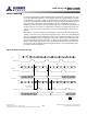
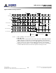

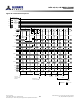
Table Of Contents
- DDR3L SDRAM
- Description
- State Diagram
- Functional Description
- Functional Block Diagrams
- Ball Assignments and Descriptions
- Package Dimensions
- Electrical Specifications
- Thermal Characteristics
- Electrical Specifications – I DD Specifications and Conditions
- Electrical Characteristics – 1.35V IDD Specifications
- Electrical Specifications – DC and AC
- ODT Characteristics
- Output Driver Impedance
- Output Characteristics and Operating Conditions
- Speed Bin Tables
- Electrical Characteristics and AC Operating Conditions
- Electrical Characteristics and AC Operating Conditions
- Command and Address Setup, Hold, and Derating
- Data Setup, Hold, and Derating
- Commands – Truth Tables
- Commands
- Input Clock Frequency Change
- Write Leveling
- Initialization
- Voltage Initialization / Change
- Mode Registers
- Mode Register 0 (MR0)
- Mode Register 1 (MR1)
- Mode Register 2 (MR2)
- Mode Register 3 (MR3)
- MODE REGISTER SET (MRS) Command
- ZQ CALIBRATION Operation
- ACTIVATE Operation
- READ Operation
- WRITE Operation
- PRECHARGE Operation
- SELF REFRESH Operation
- Extended Temperature Usage
- Power-Down Mode
- RESET Operation
- On-Die Termination (ODT)
- Dynamic ODT
- Synchronous ODT Mode
- Asynchronous ODT Mode
- Asynchronous to Synchronous ODT Mode Transition (Power-Down Exit)
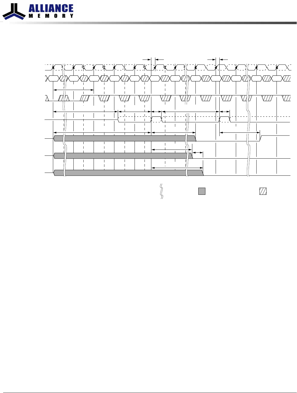
Figure 44: Write Leveling Sequence
CK
CK#
Command
T1 T2
Early remaining DQ
Late remaining DQ
t
WLOE
NOP
2
NOP
MRS
1
NOP NOP NOP NOP NOP NOP NOP NOP NOP
t
WLS
t
WLH
Don’t CareUndefined Driving Mode
Indicates break
in time scale
Prime DQ
5
Differential DQS
4
ODT
t
MOD
t
DQSL
3
t
DQSL
3
t
DQSH
3
t
DQSH
3
t
WLO
t
WLMRD
t
WLDQSEN
t
WLO
t
WLO
t
WLO
Notes:
1. MRS: Load MR1 to enter write leveling mode.
2. NOP: NOP or DES.
3. DQS, DQS# needs to fulfill minimum pulse width requirements
t
DQSH (MIN) and
t
DQSL
(MIN) as defined for regular writes. The maximum pulse width is system-dependent.
4. Differential DQS is the differential data strobe (DQS, DQS#). Timing reference points are
the zero crossings. The solid line represents DQS; the dotted line represents DQS#.
5. DRAM drives leveling feedback on a prime DQ (DQ0 for x4 and x8). The remaining DQ
are driven LOW and remain in this state throughout the leveling procedure.
8Gb: x4, x8, x16 DDR3L SDRAM
Write Leveling
124
Rev 2.0 June 2016
© 2015 Alliance Memory, Inc. All rights reserved.
Alliance Memory Inc. reserves the right to change products or specification without notice
Alliance Memory Inc. 511 Taylor Way, San Carlos, CA 94070
TEL: (650) 610-6800 FAX: (650) 620-9211