
Datasheet
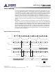
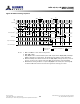

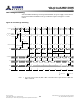
Table Of Contents
- DDR3L SDRAM
- Description
- State Diagram
- Functional Description
- Functional Block Diagrams
- Ball Assignments and Descriptions
- Package Dimensions
- Electrical Specifications
- Thermal Characteristics
- Electrical Specifications – I DD Specifications and Conditions
- Electrical Characteristics – 1.35V IDD Specifications
- Electrical Specifications – DC and AC
- ODT Characteristics
- Output Driver Impedance
- Output Characteristics and Operating Conditions
- Speed Bin Tables
- Electrical Characteristics and AC Operating Conditions
- Electrical Characteristics and AC Operating Conditions
- Command and Address Setup, Hold, and Derating
- Data Setup, Hold, and Derating
- Commands – Truth Tables
- Commands
- Input Clock Frequency Change
- Write Leveling
- Initialization
- Voltage Initialization / Change
- Mode Registers
- Mode Register 0 (MR0)
- Mode Register 1 (MR1)
- Mode Register 2 (MR2)
- Mode Register 3 (MR3)
- MODE REGISTER SET (MRS) Command
- ZQ CALIBRATION Operation
- ACTIVATE Operation
- READ Operation
- WRITE Operation
- PRECHARGE Operation
- SELF REFRESH Operation
- Extended Temperature Usage
- Power-Down Mode
- RESET Operation
- On-Die Termination (ODT)
- Dynamic ODT
- Synchronous ODT Mode
- Asynchronous ODT Mode
- Asynchronous to Synchronous ODT Mode Transition (Power-Down Exit)

Write Leveling Procedure
A memory controller initiates the DRAM write leveling mode by setting MR1[7] to 1, as-
suming the other programable features (MR0, MR1, MR2, and MR3) are first set and the
DLL is fully reset and locked. The DQ balls enter the write leveling mode going from a
High-Z state to an undefined driving state, so the DQ bus should not be driven. During
write leveling mode, only the NOP or DES commands are allowed. The memory con-
troller should attempt to level only one rank at a time; thus, the outputs of other ranks
should be disabled by setting MR1[12] to 1 in the other ranks. The memory controller
may assert ODT after a
t
MOD delay, as the DRAM will be ready to process the ODT tran-
sition. ODT should be turned on prior to DQS being driven LOW by at least ODTLon
delay (WL - 2
t
CK), provided it does not violate the aforementioned
t
MOD delay require-
ment.
The memory controller may drive DQS LOW and DQS# HIGH after
t
WLDQSEN has
been satisfied. The controller may begin to toggle DQS after
t
WLMRD (one DQS toggle
is DQS transitioning from a LOW state to a HIGH state with DQS# transitioning from a
HIGH state to a LOW state, then both transition back to their original states). At a mini-
mum, ODTLon and
t
AON must be satisfied at least one clock prior to DQS toggling.
After
t
WLMRD and a DQS LOW preamble (
t
WPRE) have been satisfied, the memory
controller may provide either a single DQS toggle or multiple DQS toggles to sample CK
for a given DQS-to-CK skew. Each DQS toggle must not violate
t
DQSL (MIN) and
t
DQSH
(MIN) specifications.
t
DQSL (MAX) and
t
DQSH (MAX) specifications are not applicable
during write leveling mode. The DQS must be able to distinguish the CK’s rising edge
within
t
WLS and
t
WLH. The prime DQ will output the CK’s status asynchronously from
the associated DQS rising edge CK capture within
t
WLO. The remaining DQ that always
drive LOW when DQS is toggling must be LOW within
t
WLOE after the first
t
WLO is sat-
isfied (the prime DQ going LOW). As previously noted, DQS is an input and not an out-
put during this process. Figure 44 (page 124) depicts the basic timing parameters for
the overall write leveling procedure.
The memory controller will most likely sample each applicable prime DQ state and de-
termine whether to increment or decrement its DQS delay setting. After the memory
controller performs enough DQS toggles to detect the CK’s 0-to-1 transition, the memo-
ry controller should lock the DQS delay setting for that DRAM. After locking the DQS
setting is locked, leveling for the rank will have been achieved, and the write leveling
mode for the rank should be disabled or reprogrammed (if write leveling of another
rank follows).
8Gb: x4, x8, x16 DDR3L SDRAM
Write Leveling
123
Rev 2.0 June 2016
© 2015 Alliance Memory, Inc. All rights reserved.
Alliance Memory Inc. reserves the right to change products or specification without notice
Alliance Memory Inc. 511 Taylor Way, San Carlos, CA 94070
TEL: (650) 610-6800 FAX: (650) 620-9211