
Datasheet
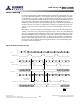
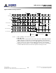

Table Of Contents
- DDR3L SDRAM
- Description
- State Diagram
- Functional Description
- Functional Block Diagrams
- Ball Assignments and Descriptions
- Package Dimensions
- Electrical Specifications
- Thermal Characteristics
- Electrical Specifications – I DD Specifications and Conditions
- Electrical Characteristics – 1.35V IDD Specifications
- Electrical Specifications – DC and AC
- ODT Characteristics
- Output Driver Impedance
- Output Characteristics and Operating Conditions
- Speed Bin Tables
- Electrical Characteristics and AC Operating Conditions
- Electrical Characteristics and AC Operating Conditions
- Command and Address Setup, Hold, and Derating
- Data Setup, Hold, and Derating
- Commands – Truth Tables
- Commands
- Input Clock Frequency Change
- Write Leveling
- Initialization
- Voltage Initialization / Change
- Mode Registers
- Mode Register 0 (MR0)
- Mode Register 1 (MR1)
- Mode Register 2 (MR2)
- Mode Register 3 (MR3)
- MODE REGISTER SET (MRS) Command
- ZQ CALIBRATION Operation
- ACTIVATE Operation
- READ Operation
- WRITE Operation
- PRECHARGE Operation
- SELF REFRESH Operation
- Extended Temperature Usage
- Power-Down Mode
- RESET Operation
- On-Die Termination (ODT)
- Dynamic ODT
- Synchronous ODT Mode
- Asynchronous ODT Mode
- Asynchronous to Synchronous ODT Mode Transition (Power-Down Exit)
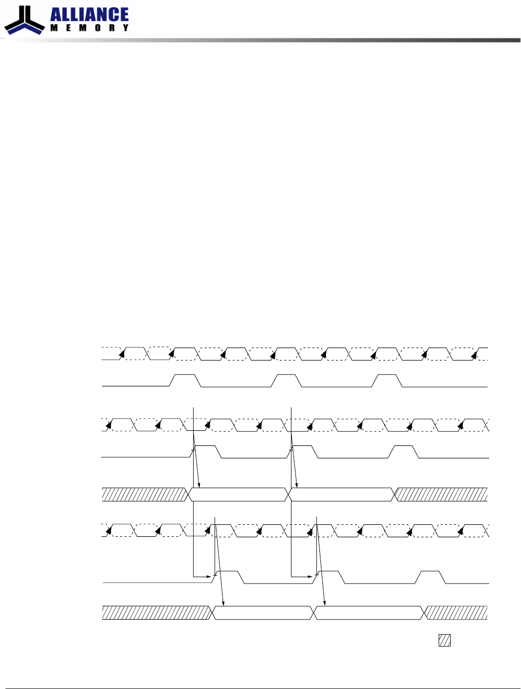
Write Leveling
For better signal integrity, DDR3 SDRAM memory modules have adopted fly-by topolo-
gy for the commands, addresses, control signals, and clocks. Write leveling is a scheme
for the memory controller to adjust or de-skew the DQS strobe (DQS, DQS#) to CK rela-
tionship at the DRAM with a simple feedback feature provided by the DRAM. Write lev-
eling is generally used as part of the initialization process, if required. For normal
DRAM operation, this feature must be disabled. This is the only DRAM operation where
the DQS functions as an input (to capture the incoming clock) and the DQ function as
outputs (to report the state of the clock). Note that nonstandard ODT schemes are re-
quired.
The memory controller using the write leveling procedure must have adjustable delay
settings on its DQS strobe to align the rising edge of DQS to the clock at the DRAM pins.
This is accomplished when the DRAM asynchronously feeds back the CK status via the
DQ bus and samples with the rising edge of DQS. The controller repeatedly delays the
DQS strobe until a CK transition from 0 to 1 is detected. The DQS delay established by
this procedure helps ensure
t
DQSS,
t
DSS, and
t
DSH specifications in systems that use
fly-by topology by de-skewing the trace length mismatch. A conceptual timing of this
procedure is shown in Figure 43.
Figure 43: Write Leveling Concept
CK
CK#
Source
Differential DQS
Differential DQS
Differential DQS
DQ
DQ
CK
CK#
Destination
Destination
Push DQS to capture
0–1 transition
T0 T1 T2 T3 T4 T5 T6 T7
T0 T1 T2 T3 T4 T5 T6Tn
CK
CK#
T0 T1 T2 T3 T4 T5 T6Tn
Don’t Care
11
00
8Gb: x4, x8, x16 DDR3L SDRAM
Write Leveling
121
Rev 2.0 June 2016
© 2015 Alliance Memory, Inc. All rights reserved.
Alliance Memory Inc. reserves the right to change products or specification without notice
Alliance Memory Inc. 511 Taylor Way, San Carlos, CA 94070
TEL: (650) 610-6800 FAX: (650) 620-9211