
Datasheet
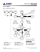
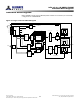
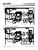
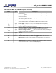
Table Of Contents
- DDR3L SDRAM
- Description
- State Diagram
- Functional Description
- Functional Block Diagrams
- Ball Assignments and Descriptions
- Package Dimensions
- Electrical Specifications
- Thermal Characteristics
- Electrical Specifications – I DD Specifications and Conditions
- Electrical Characteristics – 1.35V IDD Specifications
- Electrical Specifications – DC and AC
- ODT Characteristics
- Output Driver Impedance
- Output Characteristics and Operating Conditions
- Speed Bin Tables
- Electrical Characteristics and AC Operating Conditions
- Electrical Characteristics and AC Operating Conditions
- Command and Address Setup, Hold, and Derating
- Data Setup, Hold, and Derating
- Commands – Truth Tables
- Commands
- Input Clock Frequency Change
- Write Leveling
- Initialization
- Voltage Initialization / Change
- Mode Registers
- Mode Register 0 (MR0)
- Mode Register 1 (MR1)
- Mode Register 2 (MR2)
- Mode Register 3 (MR3)
- MODE REGISTER SET (MRS) Command
- ZQ CALIBRATION Operation
- ACTIVATE Operation
- READ Operation
- WRITE Operation
- PRECHARGE Operation
- SELF REFRESH Operation
- Extended Temperature Usage
- Power-Down Mode
- RESET Operation
- On-Die Termination (ODT)
- Dynamic ODT
- Synchronous ODT Mode
- Asynchronous ODT Mode
- Asynchronous to Synchronous ODT Mode Transition (Power-Down Exit)

State Diagram
Figure 2: Simplified State Diagram
SRX = Self refresh exit
WRITE = WR, WRS4, WRS8
WRITE AP = WRAP, WRAPS4, WRAPS8
ZQCL = ZQ LONG CALIBRATION
ZQCS = ZQ SHORT CALIBRATION
Bank
active
ReadingWriting
Activating
Refreshing
Self
refresh
Idle
Active
power-
down
ZQ
calibration
From any
state
Power
applied
Reset
procedure
Power
on
Initial-
ization
MRS, MPR,
write
leveling
Precharge
power-
down
Writing Reading
Automatic
sequence
Command
sequence
Precharging
READ
READ
READ
READ AP
READ AP
READ AP
PRE, PREA
PRE, PREA PRE, PREA
WRITE
WRITE
CKE L CKE L
CKE L
WRITE
WRITE AP
WRITE AP
WRITE AP
PDE
PDE
PDX
PDX
SRX
SRE
REF
MRS
ACT
RESET
ZQCL
ZQCL/ZQCS
ACT = ACTIVATE
MPR = Multipurpose register
MRS = Mode register set
PDE = Power-down entry
PDX = Power-down exit
PRE = PRECHARGE
PREA = PRECHARGE ALL
READ = RD, RDS4, RDS8
READ AP = RDAP, RDAPS4, RDAPS8
REF = REFRESH
RESET = START RESET PROCEDURE
SRE = Self refresh entry
8Gb: x4, x8, x16 DDR3L SDRAM
State Diagram
11
Rev 2.0 June 2016
© 2015 Alliance Memory, Inc. All rights reserved.
Alliance Memory Inc. reserves the right to change products or specification without notice
Alliance Memory Inc. 511 Taylor Way, San Carlos, CA 94070
TEL: (650) 610-6800 FAX: (650) 620-9211