
Datasheet
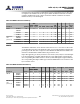
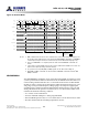
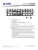

Table Of Contents
- DDR3L SDRAM
- Description
- State Diagram
- Functional Description
- Functional Block Diagrams
- Ball Assignments and Descriptions
- Package Dimensions
- Electrical Specifications
- Thermal Characteristics
- Electrical Specifications – I DD Specifications and Conditions
- Electrical Characteristics – 1.35V IDD Specifications
- Electrical Specifications – DC and AC
- ODT Characteristics
- Output Driver Impedance
- Output Characteristics and Operating Conditions
- Speed Bin Tables
- Electrical Characteristics and AC Operating Conditions
- Electrical Characteristics and AC Operating Conditions
- Command and Address Setup, Hold, and Derating
- Data Setup, Hold, and Derating
- Commands – Truth Tables
- Commands
- Input Clock Frequency Change
- Write Leveling
- Initialization
- Voltage Initialization / Change
- Mode Registers
- Mode Register 0 (MR0)
- Mode Register 1 (MR1)
- Mode Register 2 (MR2)
- Mode Register 3 (MR3)
- MODE REGISTER SET (MRS) Command
- ZQ CALIBRATION Operation
- ACTIVATE Operation
- READ Operation
- WRITE Operation
- PRECHARGE Operation
- SELF REFRESH Operation
- Extended Temperature Usage
- Power-Down Mode
- RESET Operation
- On-Die Termination (ODT)
- Dynamic ODT
- Synchronous ODT Mode
- Asynchronous ODT Mode
- Asynchronous to Synchronous ODT Mode Transition (Power-Down Exit)
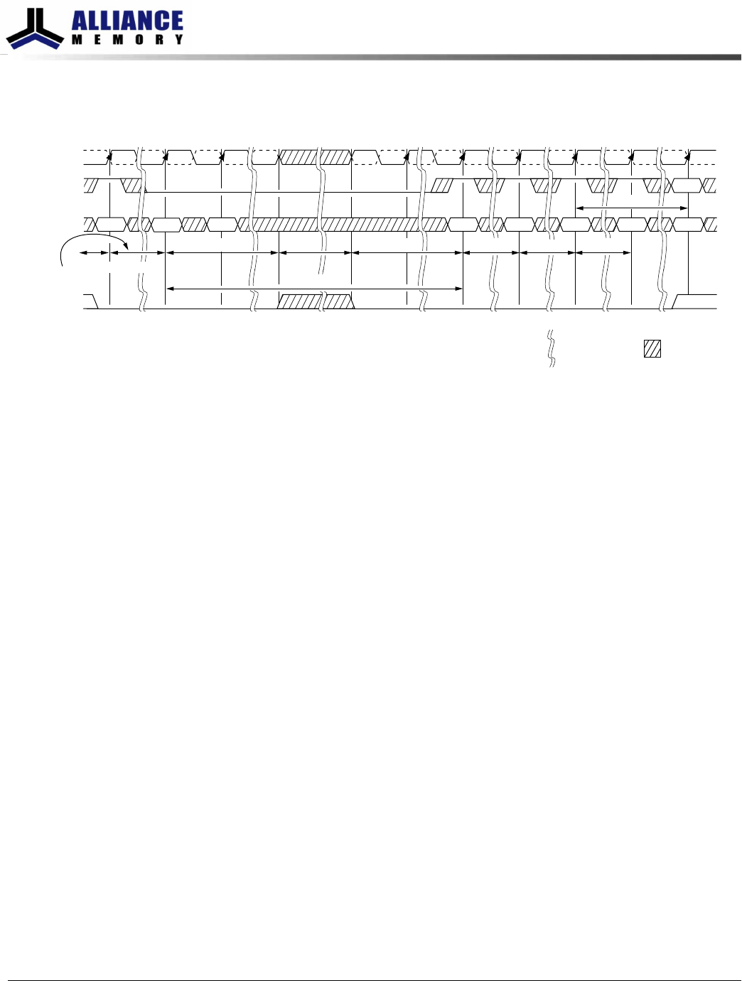
Figure 40: DLL Disable Mode to DLL Enable Mode
CKE
T0 Ta0 Ta1 Tb0 Tc0 Tc1 Td0 Te0 Tf0 Tg0
CK
CK#
ODT
10
SRE
1
NOP
Command
NOP
SRX
2
MRS
3
MRS
4
MRS
5
Valid
6
Valid
Don’t Care
Indicates break
in time scale
t
CKSRE
t
CKSRX
987
t
XS
t
MRD
t
MRD
t
CKESR
ODTLoff + 1 ×
t
CK
Th0
t
DLLK
Notes:
1. Enter SELF REFRESH.
2. Exit SELF REFRESH.
3. Wait
t
XS, then set MR1[0] to 0 to enable DLL.
4. Wait
t
MRD, then set MR0[8] to 1 to begin DLL RESET.
5. Wait
t
MRD, update registers (CL, CWL, and write recovery may be necessary).
6. Wait
t
MOD, any valid command.
7. Starting with the idle state.
8. Change frequency.
9. Clock must be stable at least
t
CKSRX.
10. Static LOW in the case that R
TT,nom
or R
TT(WR)
is enabled; otherwise, static LOW or HIGH.
The clock frequency range for the DLL disable mode is specified by the parameter
t
CK
(DLL_DIS). Due to latency counter and timing restrictions, only CL = 6 and CWL = 6 are
supported.
DLL disable mode will affect the read data clock to data strobe relationship (
t
DQSCK)
but not the data strobe to data relationship (
t
DQSQ,
t
QH). Special attention is needed to
line up read data to the controller time domain.
Compared to the DLL on mode where
t
DQSCK starts from the rising clock edge AL + CL
cycles after the READ command, the DLL disable mode
t
DQSCK starts AL + CL - 1 cycles
after the READ command.
WRITE operations function similarly between the DLL enable and DLL disable modes;
however, ODT functionality is not allowed with DLL disable mode.
8Gb: x4, x8, x16 DDR3L SDRAM
Commands
117
Rev 2.0 June 2016
© 2015 Alliance Memory, Inc. All rights reserved.
Alliance Memory Inc. reserves the right to change products or specification without notice
Alliance Memory Inc. 511 Taylor Way, San Carlos, CA 94070
TEL: (650) 610-6800 FAX: (650) 620-9211