
Datasheet
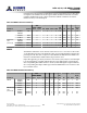
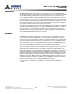
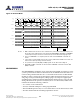
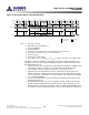

Table Of Contents
- DDR3L SDRAM
- Description
- State Diagram
- Functional Description
- Functional Block Diagrams
- Ball Assignments and Descriptions
- Package Dimensions
- Electrical Specifications
- Thermal Characteristics
- Electrical Specifications – I DD Specifications and Conditions
- Electrical Characteristics – 1.35V IDD Specifications
- Electrical Specifications – DC and AC
- ODT Characteristics
- Output Driver Impedance
- Output Characteristics and Operating Conditions
- Speed Bin Tables
- Electrical Characteristics and AC Operating Conditions
- Electrical Characteristics and AC Operating Conditions
- Command and Address Setup, Hold, and Derating
- Data Setup, Hold, and Derating
- Commands – Truth Tables
- Commands
- Input Clock Frequency Change
- Write Leveling
- Initialization
- Voltage Initialization / Change
- Mode Registers
- Mode Register 0 (MR0)
- Mode Register 1 (MR1)
- Mode Register 2 (MR2)
- Mode Register 3 (MR3)
- MODE REGISTER SET (MRS) Command
- ZQ CALIBRATION Operation
- ACTIVATE Operation
- READ Operation
- WRITE Operation
- PRECHARGE Operation
- SELF REFRESH Operation
- Extended Temperature Usage
- Power-Down Mode
- RESET Operation
- On-Die Termination (ODT)
- Dynamic ODT
- Synchronous ODT Mode
- Asynchronous ODT Mode
- Asynchronous to Synchronous ODT Mode Transition (Power-Down Exit)
precharge is not selected, the row will remain open for subsequent accesses. The value
on input A12 (if enabled in the mode register) when the READ command is issued de-
termines whether BC4 (chop) or BL8 is used. After a READ command is issued, the
READ burst may not be interrupted.
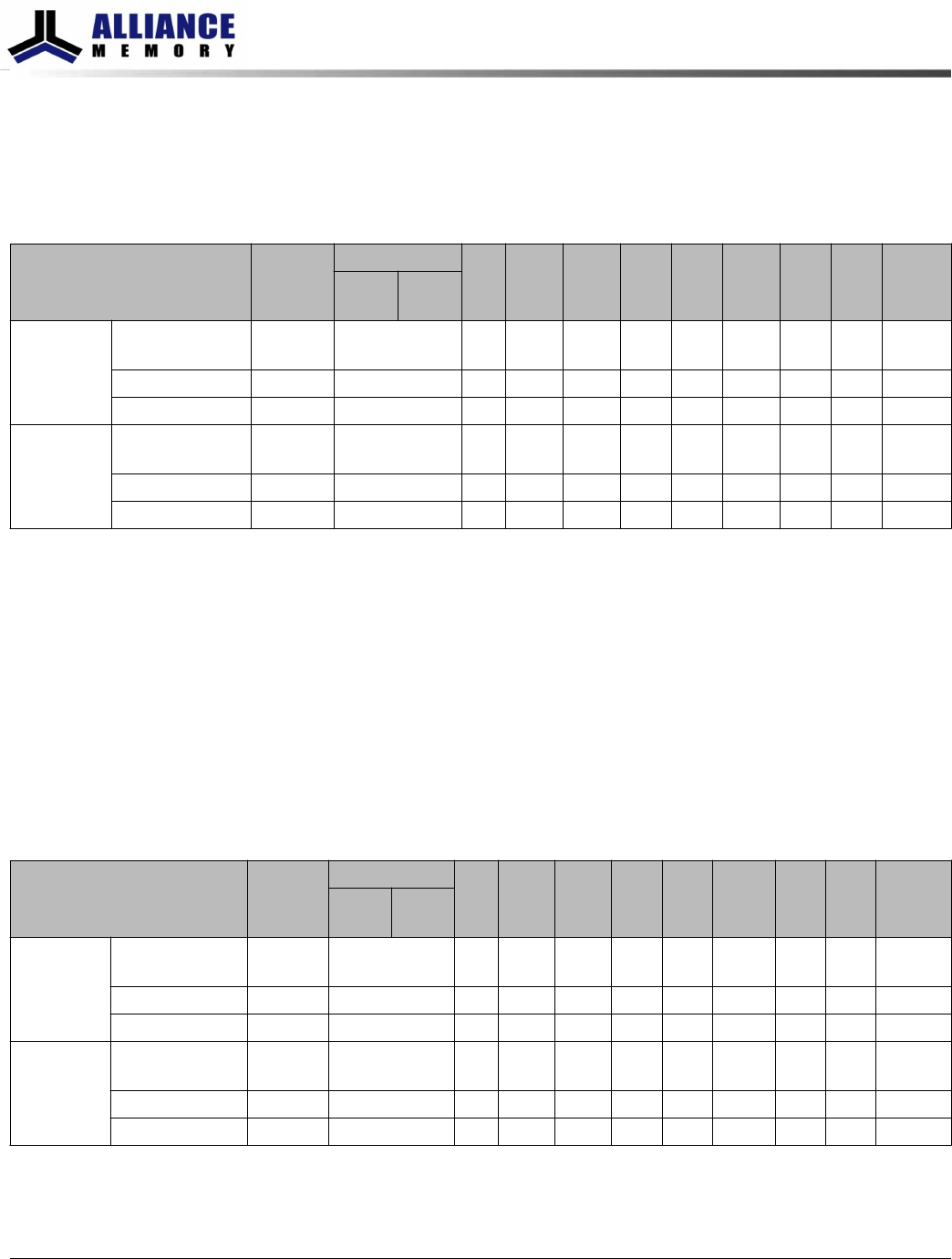
Table 69: READ Command Summary
Function Symbol
CKE
CS# RAS# CAS# WE#
BA
[2:0]
An A12 A10
A[11,
9:0]
Prev.
Cycle
Next
Cycle
READ BL8MRS,
BC4MRS
RD H L H L H BA RFU V L CA
BC4OTF RDS4 H L H L H BA RFU L L CA
BL8OTF RDS8 H L H L H BA RFU H L CA
READ with
auto
precharge
BL8MRS,
BC4MRS
RDAP H L H L H BA RFU V H CA
BC4OTF RDAPS4 H L H L H BA RFU L H CA
BL8OTF RDAPS8 H L H L H BA RFU H H CA
WRITE
The WRITE command is used to initiate a burst write access to an active row. The value
on the BA[2:0] inputs selects the bank. The value on input A10 determines whether auto
precharge is used. The value on input A12 (if enabled in the MR) when the WRITE com-
mand is issued determines whether BC4 (chop) or BL8 is used.
Input data appearing on the DQ is written to the memory array subject to the DM input
logic level appearing coincident with the data. If a given DM signal is registered LOW,
the corresponding data will be written to memory. If the DM signal is registered HIGH,
the corresponding data inputs will be ignored and a WRITE will not be executed to that
byte/column location.
Table 70: WRITE Command Summary
Function Symbol
CKE
CS# RAS# CAS# WE#
BA
[2:0]
An A12 A10
A[11,
9:0]
Prev.
Cycle
Next
Cycle
WRITE BL8MRS,
BC4MRS
WR H L H L L BA RFU V L CA
BC4OTF WRS4 H L H L L BA RFU L L CA
BL8OTF WRS8 H L H L L BA RFU H L CA
WRITE with
auto
precharge
BL8MRS,
BC4MRS
WRAP H L H L L BA RFU V H CA
BC4OTF WRAPS4 H L H L L BA RFU L H CA
BL8OTF WRAPS8 H L H L L BA RFU H H CA
8Gb: x4, x8, x16 DDR3L SDRAM
Commands
112
Rev 2.0 June 2016
© 2015 Alliance Memory, Inc. All rights reserved.
Alliance Memory Inc. reserves the right to change products or specification without notice
Alliance Memory Inc. 511 Taylor Way, San Carlos, CA 94070
TEL: (650) 610-6800 FAX: (650) 620-9211