
Datasheet
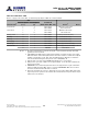
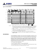
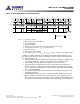

Table Of Contents
- DDR3L SDRAM
- Description
- State Diagram
- Functional Description
- Functional Block Diagrams
- Ball Assignments and Descriptions
- Package Dimensions
- Electrical Specifications
- Thermal Characteristics
- Electrical Specifications – I DD Specifications and Conditions
- Electrical Characteristics – 1.35V IDD Specifications
- Electrical Specifications – DC and AC
- ODT Characteristics
- Output Driver Impedance
- Output Characteristics and Operating Conditions
- Speed Bin Tables
- Electrical Characteristics and AC Operating Conditions
- Electrical Characteristics and AC Operating Conditions
- Command and Address Setup, Hold, and Derating
- Data Setup, Hold, and Derating
- Commands – Truth Tables
- Commands
- Input Clock Frequency Change
- Write Leveling
- Initialization
- Voltage Initialization / Change
- Mode Registers
- Mode Register 0 (MR0)
- Mode Register 1 (MR1)
- Mode Register 2 (MR2)
- Mode Register 3 (MR3)
- MODE REGISTER SET (MRS) Command
- ZQ CALIBRATION Operation
- ACTIVATE Operation
- READ Operation
- WRITE Operation
- PRECHARGE Operation
- SELF REFRESH Operation
- Extended Temperature Usage
- Power-Down Mode
- RESET Operation
- On-Die Termination (ODT)
- Dynamic ODT
- Synchronous ODT Mode
- Asynchronous ODT Mode
- Asynchronous to Synchronous ODT Mode Transition (Power-Down Exit)
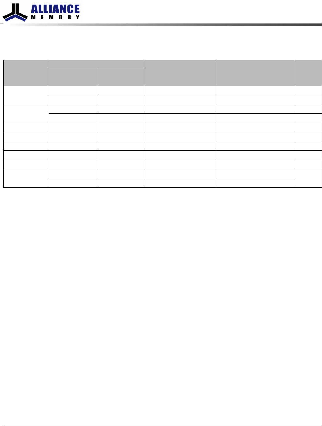
Table 68: Truth Table – CKE
Notes 1–2 apply to the entire table; see Table 67 (page 108) for additional command details
Current State
3
CKE
Command
5
(RAS#, CAS#, WE#, CS#) Action
5
Notes
Previous Cycle
4
(n - 1)
Present Cycle
4
(n)
Power-down L L “Don’t Care” Maintain power-down
L H DES or NOP Power-down exit
Self refresh L L “Don’t Care” Maintain self refresh
L H DES or NOP Self refresh exit
Bank(s) active H L DES or NOP Active power-down entry
Reading H L DES or NOP Power-down entry
Writing H L DES or NOP Power-down entry
Precharging H L DES or NOP Power-down entry
Refreshing H L DES or NOP Precharge power-down entry
All banks idle H L DES or NOP Precharge power-down entry 6
H L REFRESH Self refresh
Notes:
1. All states and sequences not shown are illegal or reserved unless explicitly described
elsewhere in this document.
2.
t
CKE (MIN) means CKE must be registered at multiple consecutive positive clock edges.
CKE must remain at the valid input level the entire time it takes to achieve the required
number of registration clocks. Thus, after any CKE transition, CKE may not transition
from its valid level during the time period of
t
IS +
t
CKE (MIN) +
t
IH.
3. Current state = The state of the DRAM immediately prior to clock edge n.
4. CKE (n) is the logic state of CKE at clock edge n; CKE (n - 1) was the state of CKE at the
previous clock edge.
5. COMMAND is the command registered at the clock edge (must be a legal command as
defined in Table 67 (page 108)). Action is a result of COMMAND. ODT does not affect
the states described in this table and is not listed.
6. Idle state = All banks are closed, no data bursts are in progress, CKE is HIGH, and all tim-
ings from previous operations are satisfied. All self refresh exit and power-down exit pa-
rameters are also satisfied.
8Gb: x4, x8, x16 DDR3L SDRAM
Commands – Truth Tables
110
Rev 2.0 June 2016
© 2015 Alliance Memory, Inc. All rights reserved.
Alliance Memory Inc. reserves the right to change products or specification without notice
Alliance Memory Inc. 511 Taylor Way, San Carlos, CA 94070
TEL: (650) 610-6800 FAX: (650) 620-9211