
Datasheet
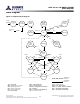
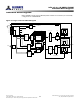
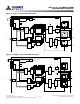
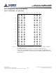
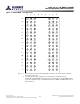
Table Of Contents
- DDR3L SDRAM
- Description
- State Diagram
- Functional Description
- Functional Block Diagrams
- Ball Assignments and Descriptions
- Package Dimensions
- Electrical Specifications
- Thermal Characteristics
- Electrical Specifications – I DD Specifications and Conditions
- Electrical Characteristics – 1.35V IDD Specifications
- Electrical Specifications – DC and AC
- ODT Characteristics
- Output Driver Impedance
- Output Characteristics and Operating Conditions
- Speed Bin Tables
- Electrical Characteristics and AC Operating Conditions
- Electrical Characteristics and AC Operating Conditions
- Command and Address Setup, Hold, and Derating
- Data Setup, Hold, and Derating
- Commands – Truth Tables
- Commands
- Input Clock Frequency Change
- Write Leveling
- Initialization
- Voltage Initialization / Change
- Mode Registers
- Mode Register 0 (MR0)
- Mode Register 1 (MR1)
- Mode Register 2 (MR2)
- Mode Register 3 (MR3)
- MODE REGISTER SET (MRS) Command
- ZQ CALIBRATION Operation
- ACTIVATE Operation
- READ Operation
- WRITE Operation
- PRECHARGE Operation
- SELF REFRESH Operation
- Extended Temperature Usage
- Power-Down Mode
- RESET Operation
- On-Die Termination (ODT)
- Dynamic ODT
- Synchronous ODT Mode
- Asynchronous ODT Mode
- Asynchronous to Synchronous ODT Mode Transition (Power-Down Exit)

Table 51: DDR3L-1333 Speed Bins .................................................................................................................. 69
Table 52: DDR3L-1600 Speed Bins .................................................................................................................. 70
Table 53: DDR3L-1866 Speed Bins .................................................................................................................. 71
Table 54: DDR3L-2133 Speed Bins .................................................................................................................. 72
Table 55: Electrical Characteristics and AC Operating Conditions .................................................................... 73
Table 56: Electrical Characteristics and AC Operating Conditions for Speed Extensions .................................... 83
Table 57: DDR3L Command and Address Setup and Hold Values 1 V/ns Referenced – AC/DC-Based ................ 93
Table 58: DDR3L-800/1066 Derating Values
t
IS/
t
IH – AC160/DC90-Based ........................................................ 94
Table 59: DDR3L-800/1066/1333/1600 Derating Values for
t
IS/
t
IH – AC135/DC90-Based ................................. 94
Table 60: DDR3L-1866/2133 Derating Values for
t
IS/
t
IH – AC125/DC90-Based ................................................. 94
Table 61: DDR3L Minimum Required Time
t
VAC Above V
IH(AC)
(Below V
IL[AC]
) for Valid ADD/CMD Transition .. 95
Table 62: DDR3L Data Setup and Hold Values at 1 V/ns (DQS, DQS# at 2 V/ns) – AC/DC-Based ....................... 100
Table 63: DDR3L Derating Values for
t
DS/
t
DH – AC160/DC90-Based .............................................................. 101
Table 64: DDR3L Derating Values for
t
DS/
t
DH – AC135/DC90-Based .............................................................. 101
Table 65: DDR3L Derating Values for
t
DS/
t
DH – AC130/DC90-Based at 2V/ns ................................................. 102
Table 66: DDR3L Minimum Required Time
t
VAC Above V
IH(AC)
(Below V
IL(AC)
) for Valid DQ Transition ............. 103
Table 67: Truth Table – Command ................................................................................................................. 108
Table 68: Truth Table – CKE .......................................................................................................................... 110
Table 69: READ Command Summary ............................................................................................................ 112
Table 70: WRITE Command Summary .......................................................................................................... 112
Table 71: READ Electrical Characteristics, DLL Disable Mode ......................................................................... 118
Table 72: Write Leveling Matrix ..................................................................................................................... 122
Table 73: Burst Order .................................................................................................................................... 133
Table 74: MPR Functional Description of MR3 Bits ........................................................................................ 142
Table 75: MPR Readouts and Burst Order Bit Mapping ................................................................................... 143
Table 76: Self Refresh Temperature and Auto Self Refresh Description ............................................................ 176
Table 77: Self Refresh Mode Summary ........................................................................................................... 176
Table 78: Command to Power-Down Entry Parameters .................................................................................. 177
Table 79: Power-Down Modes ....................................................................................................................... 178
Table 80: Truth Table – ODT (Nominal) ......................................................................................................... 188
Table 81: ODT Parameters ............................................................................................................................ 188
Table 82: Write Leveling with Dynamic ODT Special Case .............................................................................. 189
Table 83: Dynamic ODT Specific Parameters ................................................................................................. 190
Table 84: Mode Registers for R
TT,nom
............................................................................................................. 190
Table 85: Mode Registers for R
TT(WR)
............................................................................................................. 191
Table 86: Timing Diagrams for Dynamic ODT ................................................................................................ 191
Table 87: Synchronous ODT Parameters ........................................................................................................ 196
Table 88: Asynchronous ODT Timing Parameters for All Speed Bins ............................................................... 201
Table 89: ODT Parameters for Power-Down (DLL Off) Entry and Exit Transition Period ................................... 203
8Gb: x4, x8, x16 DDR3L SDRAM
Description
10
Rev 2.0 June 2016
© 2015 Alliance Memory, Inc. All rights reserved.
Alliance Memory Inc. reserves the right to change products or specification without notice
Alliance Memory Inc. 511 Taylor Way, San Carlos, CA 94070
TEL: (650) 610-6800 FAX: (650) 620-9211