
Datasheet
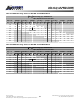
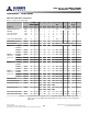
Table Of Contents
- DDR3L SDRAM
- Description
- State Diagram
- Functional Description
- Functional Block Diagrams
- Ball Assignments and Descriptions
- Package Dimensions
- Electrical Specifications
- Thermal Characteristics
- Electrical Specifications – I DD Specifications and Conditions
- Electrical Characteristics – 1.35V IDD Specifications
- Electrical Specifications – DC and AC
- ODT Characteristics
- Output Driver Impedance
- Output Characteristics and Operating Conditions
- Speed Bin Tables
- Electrical Characteristics and AC Operating Conditions
- Electrical Characteristics and AC Operating Conditions
- Command and Address Setup, Hold, and Derating
- Data Setup, Hold, and Derating
- Commands – Truth Tables
- Commands
- Input Clock Frequency Change
- Write Leveling
- Initialization
- Voltage Initialization / Change
- Mode Registers
- Mode Register 0 (MR0)
- Mode Register 1 (MR1)
- Mode Register 2 (MR2)
- Mode Register 3 (MR3)
- MODE REGISTER SET (MRS) Command
- ZQ CALIBRATION Operation
- ACTIVATE Operation
- READ Operation
- WRITE Operation
- PRECHARGE Operation
- SELF REFRESH Operation
- Extended Temperature Usage
- Power-Down Mode
- RESET Operation
- On-Die Termination (ODT)
- Dynamic ODT
- Synchronous ODT Mode
- Asynchronous ODT Mode
- Asynchronous to Synchronous ODT Mode Transition (Power-Down Exit)

Data Setup, Hold, and Derating
The total
t
DS (setup time) and
t
DH (hold time) required is calculated by adding the data
sheet
t
DS (base) and
t
DH (base) values (see Table 62 (page 100); values come from the
Electrical Characteristics and AC Operating Conditions table) to the Δ
t
DS and Δ
t
DH de-
rating values (see Table 63 (page 101), Table 64 (page 101), or Table 65 (page 102)) re-
spectively. Example:
t
DS (total setup time) =
t
DS (base) + Δ
t
DS. For a valid transition, the
input signal has to remain above/below V
IH(AC)
/V
IL(AC)
for some time
t
VAC (see Table 66
(page 103)).
Although the total setup time for slow slew rates might be negative (for example, a valid
input signal will not have reached V
IH(AC)
/V
IL(AC)
) at the time of the rising clock transi-
tion), a valid input signal is still required to complete the transition and to reach
V
IH
/V
IL(AC)
. For slew rates that fall between the values listed in Table 63 (page 101), Ta-
ble 64 (page 101), or Table 65 (page 102), the derating values may obtained by linear
interpolation.
Setup (
t
DS) nominal slew rate for a rising signal is defined as the slew rate between the
last crossing of V
REF(DC)
and the first crossing of V
IH(AC)min
. Setup (
t
DS) nominal slew
rate for a falling signal is defined as the slew rate between the last crossing of V
REF(DC)
and the first crossing of V
IL(AC)max
. If the actual signal is always earlier than the nominal
slew rate line between the shaded V
REF(DC)
-to-AC region, use the nominal slew rate for
derating value (see Figure 34 (page 104)). If the actual signal is later than the nominal
slew rate line anywhere between the shaded V
REF(DC)
-to-AC region, the slew rate of a
tangent line to the actual signal from the AC level to the DC level is used for derating
value (see Figure 36 (page 106)).
Hold (
t
DH) nominal slew rate for a rising signal is defined as the slew rate between the
last crossing of V
IL(DC)max
and the first crossing of V
REF(DC)
. Hold (
t
DH) nominal slew
rate for a falling signal is defined as the slew rate between the last crossing of V
IH(DC)min
and the first crossing of V
REF(DC)
. If the actual signal is always later than the nominal
slew rate line between the shaded DC-to-V
REF(DC)
region, use the nominal slew rate for
derating value (see Figure 35 (page 105)). If the actual signal is earlier than the nominal
slew rate line anywhere between the shaded DC-to-V
REF(DC)
region, the slew rate of a
tangent line to the actual signal from the DC-to-V
REF(DC)
region is used for derating val-
ue (see Figure 37 (page 107)).
Table 62: DDR3L Data Setup and Hold Values at 1 V/ns (DQS, DQS# at 2 V/ns) – AC/DC-Based
Symbol 800 1066 1333 1600 1866 2133 Unit Reference
t
DS (base) AC160 90 40 – – – – ps V
IH(AC)
/V
IL(AC)
t
DS (base) AC135 140 90 45 25 – – ps
t
DS (base) AC130 - - - - 70 55 ps
t
DH (base) DC90 160 110 75 55 – – ps
t
DH (base) DC90 – – – – 75 60 ps
Slew Rate Referenced 1 1 1 1 2 2 V/ns
8Gb: x4, x8, x16 DDR3L SDRAM
Data Setup, Hold, and Derating
100
Rev 2.0 June 2016
© 2015 Alliance Memory, Inc. All rights reserved.
Alliance Memory Inc. reserves the right to change products or specification without notice
Alliance Memory Inc. 511 Taylor Way, San Carlos, CA 94070
TEL: (650) 610-6800 FAX: (650) 620-9211