
Datasheet


Table Of Contents
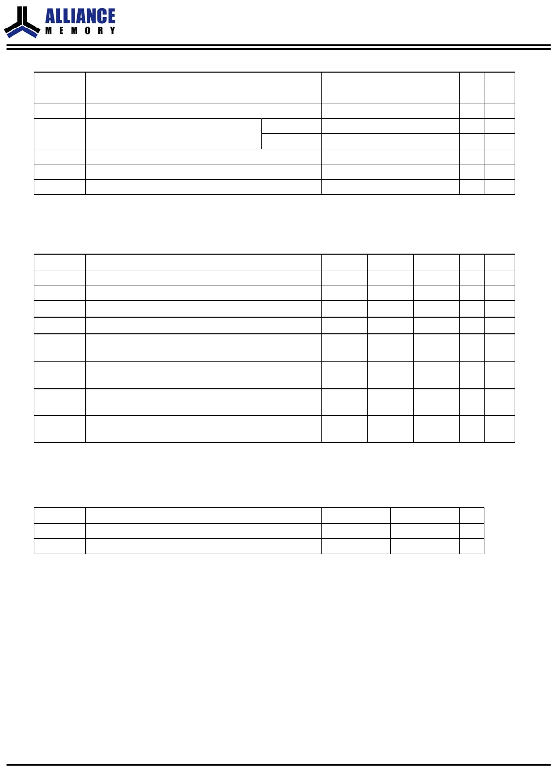
Table 13. Absolute Maximum Rating
Symbol
Item
- 5/6/7
Unit
Note
V
IN
, V
OUT
Input, Output Voltage
- 1.0 ~ 4.6
V
1
V
DD
, V
DDQ
Power Supply Voltage
-1.0 ~ 4.6
V
1
T
A
Ambient Temperature
Commercial
0 ~ 70
°C
1
Industrial
-40 ~ 85
°C
1
T
STG
Storage Temperature
- 55 ~ 150
°C
1
P
D
Power Dissipation
1
W
1
I
OS
Short Circuit Output Current
50
mA
1
Table 14. Recommended D.C. Operating Conditions
(T
A
= -40~85°C)
Symbol
Parameter
Min.
Typ.
Max.
Unit
Note
V
DD
Power Supply Voltage
3.0
3.3
3.6
V
2
V
DDQ
Power Supply Voltage(for I/O Buffer)
3.0
3.3
3.6
V
2
V
IH
LVTTL Input High Voltage
2.0
-
V
DDQ
+0.3
V
2
V
IL
LVTTL Input Low Voltage
- 0.3
-
0.8
V
2
I
IL
Input Leakage Current
( 0V V
IN
V
DD
, All other pins not under test = 0V )
- 10
-
10
A
I
OL
Output Leakage Current
Output disable, 0V V
OUT
V
DDQ
)
- 10
-
10
A
V
OH
LVTTL Output "H" Level Voltage
( I
OUT
= -2mA )
2.4
-
-
V
V
OL
LVTTL Output "L" Level Voltage
( I
OUT
= 2mA )
-
-
0.4
V
Table 15. Capacitance
(V
DD
= 3.3V, f = 1MHz, T
A
= 25°C)
Symbol
Parameter
Min.
Max.
Unit
C
I
Input Capacitance
1
4
pF
C
I/O
Input/Output Capacitance
2
5
pF
Note: These parameters are periodically sampled and are not 100% tested.
AS4C4M16SA-C&I
Confidential
- 18 of 56 -
Rev.5.0 October 2018