
Datasheet


Table Of Contents
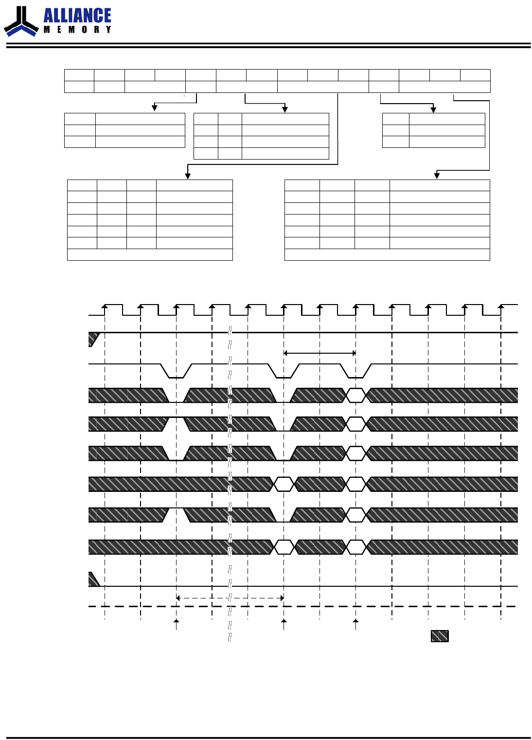
Table 5. Mode Register Bitmap
BA1
BA0
A11
A10
A9
A8
A7
A6
A5
A4
A3
A2
A1
A0
RFU*
0
RFU*
WBL
Test Mode
CAS Latency
BT
Burst Length
A9
Write Burst Length
A8
A7
Test Mode
A3
Burst Type
0
Burst
0
0
Normal
0
Sequential
1
Single Bit
1
0
Vendor Use Only
1
Interleave
0
1
Vendor Use Only
A6
A5
A4
CAS Latency
A2
A1
A0
Burst Length
0
0
0
Reserved
0
0
0
1
0
0
1
Reserved
0
0
1
2
0
1
0
2 clocks
0
1
0
4
0
1
1
3 clocks
0
1
1
8
1
0
0
Reserved
1
1
1
Full Page (Sequential)
All other Reserved
All other Reserved
*Note: RFU (Reserved for future use) should stay “0” during MRS cycle.
CLK
CS#
T0
T1 T2 T3 T4 T5 T6 T7
CKE
Don’t Care
RAS#
t
MRD
CAS#
T8 T9 T10
WE#
BA0,1
A10
A0-A9,
A11
DQM
DQ
t
RP
PrechargeAll
Mode Register
Set Command
Any
Command
Hi-Z
Address Key
Figure 15. Mode Register Set Cycle
AS4C4M16SA-C&I
Confidential
- 13 of 56 -
Rev.5.0 October 2018