
Datasheet


Table Of Contents
6 Write command
(RAS# = "H", CAS# = "L", WE# = "L", BAs = Bank, A10 = "L", A0-A7 = Column Address)
The Write command is used to write a burst of data on consecutive clock cycles from an active row in an active
bank. The bank must be active for at least t
RCD
(min.) before the Write command is issued. During write bursts,
the first valid data-in element will be registered coincident with the Write command. Subsequent data elements
will be registered on each successive positive clock edge (refer to the following figure). The DQs remain with
high-impedance at the end of the burst unless another command is initiated. The burst length and burst
sequence are determined by the mode register, which is already programmed. A full-page burst will continue
until terminated (at the end of the page it will wrap to column 0 and continue).
CLK
DQ
T0
T1 T2 T3 T4 T5 T6
DIN A
0
DIN A
1
DIN A
2
DIN A
3
don’t care
T7 T8
COMMAND
NOP WRITE A NOP NOP NOP NOP NOP NOP NOP
The first data element and the write
are registered on the same clock edge
Figure 10. Burst Write Operation
(Burst Length = 4)
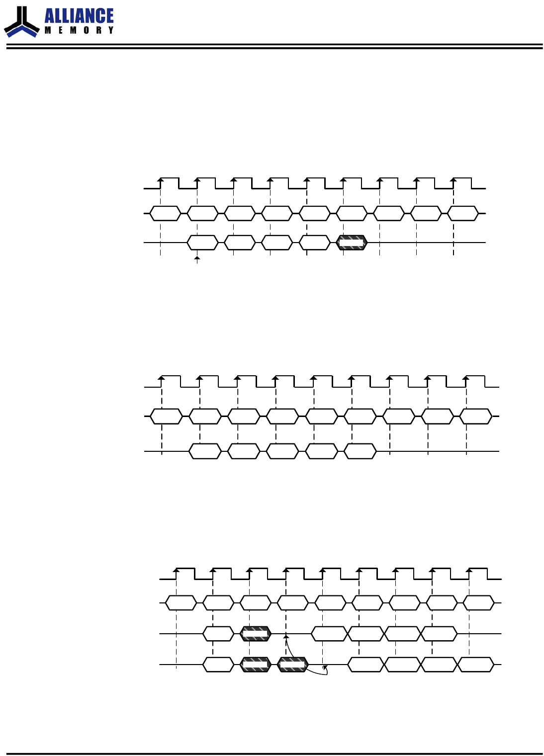
A write burst without the auto precharge function may be interrupted by a subsequent Write,
BankPrecharge/PrechargeAll, or Read command before the end of the burst length. An interrupt coming from
Write command can occur on any clock cycle following the previous Write command (refer to the following
figure).
CLK
DQ
T0 T1 T2 T3 T4 T5 T6
DIN A
0
DIN B
0
DIN B
1
DIN B
2
DIN B
3
T7 T8
COMMAND
NOP WRITE A WRITE B NOP NOP NOP NOP NOP NOP
Figure 11. Write Interrupted by a Write
(Burst Length = 4)
The Read command that interrupts a write burst without auto precharge function should be issued one cycle
after the clock edge in which the last data-in element is registered. In order to avoid data contention, input data
must be removed from the DQs at least one clock cycle before the first read data appears on the outputs (refer
to the following figure). Once the Read command is registered, the data inputs will be ignored and writes will
not be executed.
CLK
COMMAND
T0
T1 T2 T3 T4 T5 T6
NOP WRITE A READ B NOP NOP NOP NOP NOP
T7 T8
NOP
CAS# Latency=2
t
CK2
, DQ
CAS# Latency=3
t
CK3
, DQ
DOUT B
0
DOUT B
1
DOUT B
2
DOUT B
3
DOUT B
0
DOUT B
1
DOUT B
2
DOUT B
3
DIN A
0
don’t care
DIN A
0
don’t care don’t care
Input data must be removed from the DQ at
least one clock cycle before the Read data
appears on the outputs to avoid data contention
AS4C4M16SA-C&I
Confidential
- 11 of 56 -
Rev.5.0 October 2018