
Datasheet


AS4C32M16D1A-C&I
4
Rev. 1.0 Mar. /2015
Mode Register Set (MRS)
The Mode Register stores the data for controlling various operating modes of a DDR SDRAM. It programs CAS
Latency, Burst Type, and Burst Length to make the DDR SDRAM useful for a variety of applications. The default value
of the Mode Register is not defined; therefore the Mode Register must be written by the user. Values stored in the
register will be retained until the register is reprogrammed. The Mode Register is written by asserting Low on
CS
,
RAS
,
CAS
,
WE
, BA1 and BA0 (the device should have all banks idle with no bursts in progress prior to writing into
the mode register, and CKE should be High). The state of address pins A0~A12 and BA0, BA1 in the same cycle in
which
CS
,
RAS
,
CAS
and
WE
are asserted Low is written into the Mode Register. A minimum of two clock cycles,
tMRD, are required to complete the write operation in the Mode Register. The Mode Register is divided into various
fields depending on functionality. The Burst Length uses A0~A2, Burst Type uses A3, and CAS Latency (read latency
from column address) uses A4~A6. A logic 0 should be programmed to all the undefined addresses to ensure future
compatibility. Reserved states should not be used to avoid unknown device operation or incompatibility with future
versions. Refer to the table for specific codes for various burst lengths, burst types and CAS latencies.
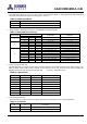
Table 4. Mode Register Bitmap
BA1
BA0
A12
A11
A10
A9
A8
A7
A6
A5
A4
A3
A2
A1
A0
Address Field
0
0
RFU must be set to “0”
T.M.
CAS Latency
BT
Burst Length
Mode Register
A8
A7
Test Mode
A6
A5
A4
CAS Latency
A3
Burst Type
A2
A1
A0
Burst Length
0
0
Normal mode
0
0
0
Reserved
0
Sequential
0
0
0
Reserved
1
0
DLL Reset
0
0
1
Reserved
1
Interleave
0
0
1
2
X
1
Test mode
0
1
0
2
0
1
0
4
0
1
1
3
0
1
1
8
BA0
Mode
1
0
0
Reserved
1
0
0
Reserved
0
MRS
1
0
1
Reserved
1
0
1
Reserved
1
EMRS
1
1
0
2.5
1
1
0
Reserved
1
1
1
Reserved
1
1
1
Reserved
Burst Length Field (A2~A0)
This field specifies the data length of column access using the A2~A0 pins and selects the Burst Length to be 2, 4, 8.
Table 5. Burst Length
A2
A1
A0
Burst Length
0
0
0
Reserved
0
0
1
2
0
1
0
4
0
1
1
8
1
0
0
Reserved
1
0
1
Reserved
1
1
0
Reserved
1
1
1
Reserved